P80C557E6 查看數據表(PDF) - Philips Electronics
零件编号
产品描述 (功能)
比赛名单
P80C557E6 Datasheet PDF : 64 Pages
| |||
Philips Semiconductors
Single-chip 8-bit microcontroller
Product specification
P83C557E6/P80C557E6
A/D Input Port Scan-Select Register ADPSS
The Special Function Register ADPSS contains control bits to select
the analog input channel(s) to be scanned for A/D conversion. The
reset value of ADPSS is (00000000). Its hardware address is E7H.
ADPSS is not bit addressable.
If all bits are ‘0’ then no A/D conversion can be started. If ADPSS is
written while an A/D conversion is in progress (ADSST in the
ADCON register is ‘1’) then the autoscan loop with the previous
selected analog inputs is completed first. The next autoscan loop is
performed with the new selected analog inputs.
A/D Result Registers ADRSLn and ADRSH:
The binary result code of A/D conversions is accessed by these
Special Function Registers. The result SFR are read only registers.
The read value after reset is indeterminate. Their data are not
affected by chip reset. They are not bit addressable.
There are 8 Special Function Registers ADRSLn
(ADRSL0...ADRSL7) – A/D Result Low byte - and one general SFR
ADRSH - A/D Result High byte - . Each of ADRSLn is associated
with the coincidently indexed analog input channel ADCn
(ADC0/P5.0...ADC7/P5.7). Reading an ADRSLn register by
software copies at the same time the two highest bits of the 10-bit
conversion result into two latches, thus preserving them until the
next read of any ADRSLn register. These two latches form bit
positions 0 and 1 of SFR ADRSH, the upper 6 bits of ADRSH are
always read as ‘0’.
Thus it is ensured to get the 10-bit result of the same single A/D
conversion by reading any register ADRSLn first and after it the
register ADRSH.
Digital Input Port Register P5
Port 5 Special Function Register P5 always represents the binary
value of the logic level at input pins P5.0/ADC0...P5.7/ADC7. P5 is
not affected by chip reset. P5 is a read only register. Its hardware
address is C7H. P5 is not bit addressable.
Reading Special Function Register P5 does not affect A/D
conversions. But it is recommended to use the digital input port
function of the hardware Port 5 only as an alternative to analog input
voltage conversions. Simultaneous mixed operation is discouraged
for the sake of A/D conversion result reliability and accuracy.
For further information on Port 5, refer to the “I/O facilities” section.
For further information on A/D Special Function Registers, refer to
the “Internal Data Memory” section.
Reset
After a RESET of the microcontroller the ADCON and ADPSS
register bits are initialized to zero. Registers ADRSLn and ADRSH
are not initialized by a RESET.
Idle and Power-down Mode
The A/D Converter is active only when the microcontroller is in
normal operating mode. If the Idle or Power-down Mode is activated,
then the ADC is switched off and put into a power saving idle state -
a conversion in progress is aborted, a previously set ADSST flag is
cleared and the internal clock is halted. The conversion result
registers are not affected.
The interrupt flag ADINT will not be set by activation of Idle or
Power-down Mode. A previously set flag ADINT will not be cleared
by the hardware. (Note: ADINT cannot be cleared by hardware at
all, except for a RESET - it must be cleared by the user software.)
After a wakeup from Idle or Power-down Mode a set flag ADINT
indicates that at least one autoscan loop was finished completely
before the microcontroller was put into the respective power
reduction mode and it indicates that the stored result data may be
fetched now - if desired.
For further information on Idle and Power-down Mode, refer to the
“Power reduction modes” section.
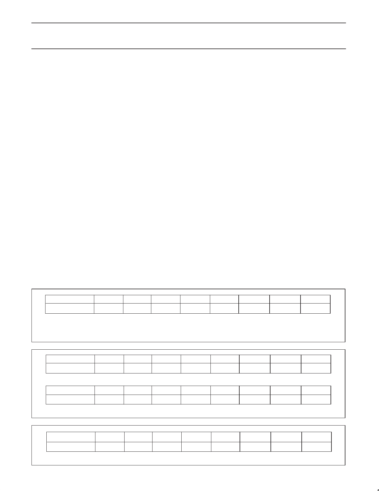
ADPSS (E7H)
7
ADPSS7
6
ADPSS6
5
ADPSS5
4
ADPSS4
3
ADPSS3
2
ADPSS2
1
ADPSS1
0
ADPSS0
ADPSS7–0 For each individual bit position:
0 = The corresponding analog input is skipped in the auto-scan loop.
1 = The corresponding analog input is included in the auto-scan loop.
Figure 16. A/D input port scan-select register.
ADRSLn
(n: 0...7)
ADRSH
7
6
5
ADRSn.7 ADRSn.6 ADRSn.5
4
3
ADRSn.4 ADRSn.3
2
ADRSn.2
1
ADRSn.1
0
ADRSn.0
7
6
5
0
0
0
4
3
0
0
Figure 17. A/D Result Registers.
2
1
0
0
ADRSn.9 ADRSn.8
P5 (C7H)
1999 Mar 02
7
P5.7
6
P5.6
5
P5.5
4
P5.4
3
P5.3
Figure 18. Digital input port register P5.
2
P5.2
20
1
P5.1
0
P5.0
Share Link: 