P80C557E6 查看數據表(PDF) - Philips Electronics
零件编号
产品描述 (功能)
比赛名单
P80C557E6 Datasheet PDF : 64 Pages
| |||
Philips Semiconductors
Single-chip 8-bit microcontroller
Product specification
P83C557E6/P80C557E6
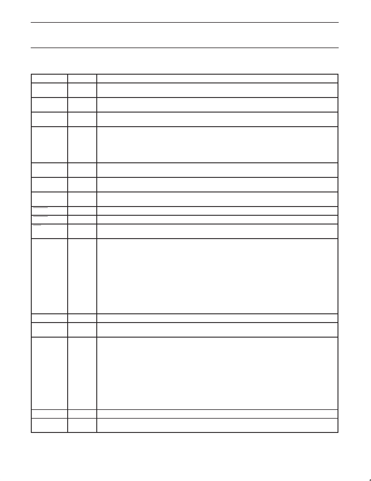
4.1 PIN DESCRIPTIONS
SYMBOL
PIN
DESCRIPTION
AVref–
1
AVref+
2
Low end of analog to digital conversion reference resistor
High end of analog to digital conversion reference resistor.
AVSS1
3
AVDD1
4
Analog ground for ADC
Analog power supply (+5 V) for ADC
AVSS2
77
AVDD2
76
Analog ground; for PLL oscillator
Analog power supply; (+5 V) for PLL oscillator
P5.7 – P5.0 5 – 12
Port 5
8–bit input port
Port pin
Alternative function
VDD1, VDD2,
VDD3, VDD4
VSS1, VSS2
VSS3, VSS4
ADEXS
14, 28,
53, 66
13, 29,
54, 67
15
PWM0
16
PWM1
17
EW
18
P4.0 – P4.7
19 – 22
24 – 27
RSTIN
30
RSTOUT
23
P1.0 – P1.7 31 – 38
P5.0–P5.7
Eight input channels to ADC (ADC0–ADC7)
Digital power supply: +5 V power supply pins during normal operation and power reduction modes. All pins
must be connected.
Digital ground: circuit ground potential. All pins must be connected.
Start ADC operation: Input starting analog to digital conversion triggered by a programmable edge (ADC
operation can also be started by software). This pin must not float
Pulse width modulation output 0
Pulse width modulation output 1
Enable watchdog timer: Enable for T3 watchdog timer and disable Power–down Mode.This pin must not
float.
Port 4
8–bit quasi–bidirectional I/O port
Port pin
Alternative function
P4.0
P4.1
P4.2
P4.3
P4.4
P4.5
P4.6
P4.7
CMSR0 }
CMSR1 }
CMSR2 } compare and set/reset
CMSR3 } outputs on a match with timer T2
CMSR4 }
CMSR5 }
CMT0 } compare and toggle outputs
CMT1 } on a match with timer T2
Reset: Input to reset the P8xC557E6.
Reset: Output of the P8xC557E6 for resetting peripheral devices during initialization and Watchdog Timer
overflow.
Port 1
8–bit quasi–bidirectional I/O port
Port pin
Alternative function
SCL
SDA
P1.0
P1.1
P1.2
P1.3
P1.4
P1.5
P1.6
P1.7
CT0I/INT2}
CT1I/INT3} :
CT2I/INT4}
CT3I/INT5}
T2
:
RT2
:
Capture timer inputs for
timer T2 or external interrupt inputs
T2 event input, rising edge triggered
T2 timer reset input, rising edge triggered
39
I2C–bus serial clock I/O port
40
I2C–bus serial data I/O port
If SCL and SDA are not used, they must be connected to VSS.
1999 Mar 02
6
Share Link: 