P80C557E6 查看數據表(PDF) - Philips Electronics
零件编号
产品描述 (功能)
比赛名单
P80C557E6 Datasheet PDF : 64 Pages
| |||
Philips Semiconductors
Single-chip 8-bit microcontroller
Product specification
P83C557E6/P80C557E6
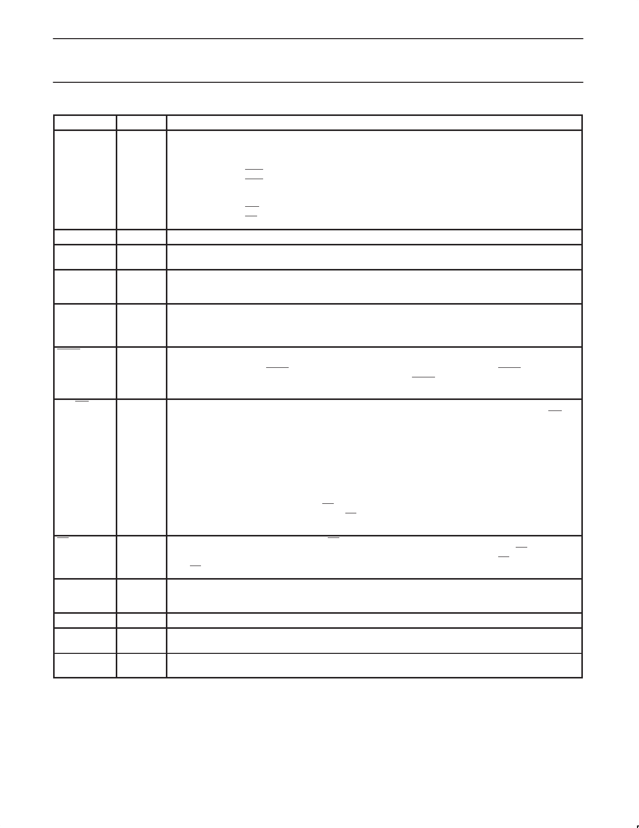
SYMBOL
P3.0 – P3.7
N.C.
XTAL2
XTAL1
P2.0 – P2.7
PIN
41 – 48
49 – 50
51
52
55 – 62
DESCRIPTION
8–bit quasi–bidirectional I/O port
Port pin
Alternative function
P3.0
RXD :
Serial input port
P3.1
TXD :
Serial output port
P3.2
INT0 :
External interrupt
P3.3
INT1 :
External interrupt
P3.4
T0
:
Timer 0 external input
P3.5
T1
:
Timer 1 external input
P3.6
WR
:
External data memory write strobe
P3.7
RD
:
External data memory read strobe
Not connected pins.
Crystal pin 2: output of the inverting amplifier that forms the oscillator. Left open–circuit when an external oscillator
clock is used.
Crystal pin 1: input to the inverting amplifier that forms the oscillator, and input to the internal clock generator.
Receives the external oscillator clock signal when an external oscillator is used. Must be connected to logic
HIGH if the PLL oscillator is selected (SELXTAL1 = LOW)
Port2: 8–bit quasi–bidirectional I/O port with internal pull–ups.During access to external memories (RAM/ROM)
that use 16–bit addresses (MOVX@DPTR) Port 2 emits the high order address byte.
PSEN
63
ALE/WE
64
Port 2 can sink/source one TTL (=4 LSTTL) input. It can drive CMOS inputs without external pull–ups.
Program Store Enable output: read strobe to the external program memory via Port 0 and 2. Is activated twice
each machine cycle during fetches from external program memory. When executing out of external program
memory two activations of PSEN are skipped during each access to external data memory. PSEN is not activated
(remains HIGH) during no fetches from external program memory. PSEN can sink/source 8 LSTTL inputs. It can
drive CMOS inputs without external pull–ups.
Address Latch Enable output: latches the low byte of the address during access of external memory in normal
operation. It is activated every six oscillator periods except during an external data memory access. ALE/WE can
sink/–source 8 LSTTL inputs.
It can drive CMOS inputs without an external pull–up.
To prohibit the toggling of ALE pin (RFI noise reduction) the bit RFI in the PCON Register (PCON.5) must be set
by software. This bit is cleared on RESET and can be set and cleared by software. When set, ALE pin will be pulled
down internally, switching an external address latch to a quiet state. The MOVX instruction will still toggle ALE if
external memory is accessed.
ALE will retain its normal high value during Idle Mode and a low value during Power–down Mode while in the “RFI”
mode. Additionally during internal access (EA = 1) ALE will toggle normally when the address exceeds the internal
program memory size. During external access (EA = 0) ALE will always toggle normally, whether the flag “RFI”
is set or not.
EA
65
External Access Input: If, during RESET, EA is held at a TTL level HIGH the CPU executes out of the
internal program memory, provided the program counter is less than 49152. If, during RESET, EA is held at a
TTL level LOW the CPU executes out of external program memory via Port 0 and Port 2. EA is not allowed to
float. EA is latched during RESET and don’t care after RESET.
P0.7–P0.0
68 –75
Port 0: 8–bit open drain bidirectional I/O port. It is also the multiplexed low–order address and data bus during
accesses to external memory (during theses accesses internal pull–ups are activated). Port 0 can sink/source 8
LSTTL inputs.
XTAL3
78
Crystal pin, output of the inverting amplifier that forms the 32 kHz oscillator
XTAL4
79
Crystal pin, input to the inverting amplifier that forms the 32 kHz oscillator. XTAL3 and XTAL4 are pulled LOW
if the PLL oscillator is not selected (SELXTAL1 = HIGH) or if Reset is active.
SELXTAL1
80
Must be connected to logic HIGH level to select the HF oscillator, using the XTAL1/XTAL2 crystal. If pulled low the
PLL is selected for clocking of the controller, using the XTAL3/ XTAL4 crystal.
NOTE:
1. To avoid a ‘latch–up’ effect at Power–on, the voltage at any pin at any time must not be higher or lower than VDD+ 0.5 V or VSS– 0.5 V
respectively.
1999 Mar 02
7
Share Link: 