LC7958NC 查看數據表(PDF) - SANYO -> Panasonic
零件编号
产品描述 (功能)
比赛名单
LC7958NC Datasheet PDF : 11 Pages
| |||
LC7958NC
The characteristics shown below are those of devices encapsulated in the SANYO standard ceramic package
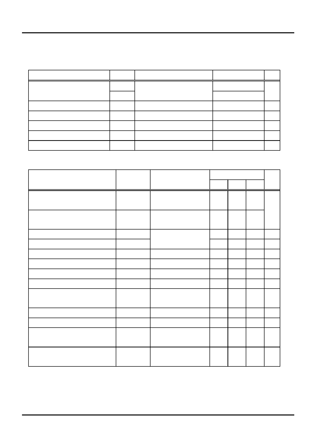
Specifications
Absolute Maximum Ratings at Vss=0V
Parameter
Symbol
Conditions
Power supply voltage
VDD1
Ta = 25 °C
VDD2
Input voltage
Output voltage
Driver output current
VI Ta = 25 °C
VO Ta = 25 °C
IOUT
Operating Junction temperature Tj
Storage temperature
Tstg
Ratings
Unit
-0.3 to 6.5
V
-0.3 to 6.5
-0.3 to VDD1+ 0.3 V
-0.3 to VDD1+ 0.3 V
0 to -10 mA
-10 to 125 °C
-35 to 125 °C
Allowable Operating Ranges at Vss = 0 V, VDD1 = VDD2 = 5 V ± 10%, Ta = 0 to 100°C
Parameter
Symbol
Conditions
Ratings
Unit
min typ max
Power supply voltage
Potential difference*1
VDD1(pad 2),
VDD1,VDD2
VDD2(pad 6)
VDF
Between VDD1 and
VDD2
4.5
5.5
V
-0.3 0 0.3
High-level input voltage
Low-level input voltage
VIH
All inputs
VIL
2.0
VDD1 V
0
0.8 V
Clock frequency
fc
CLOCK 1
10 MHz
Clock duty
D CLK CLOCK 1
35 50 65 %
Setup time from SI to CLOCK1
tsc
SI, CLOCK 1
30
ns
Hold time from CLOCK1 to SI
thold SI, CLOCK 1
10
ns
Setup time from CLOCK1 to
tSL
LOAD 1, CLOCK 1
50
ns
LOAD1
Hold time from LOAD1 to CLOCK1
tHL
LOAD 1, CLOCK 1
50
ns
LOAD1 pulse width
tWL LOAD 1
40
ns
CLOCK1 rise/fall time
tCr
CLOCK 1
tCf
35 ns
LOAD1 rise/fall time
tLr
LOAD 1
tLf
35 ns
*1:In case potential difference occurred between VDD1 and VDD2, Driver current value changes. Therefore using it with
VDD1=VDD2 is recommended.
6585-2/11
Share Link: 