LC7958NC 查看數據表(PDF) - SANYO -> Panasonic
零件编号
产品描述 (功能)
比赛名单
LC7958NC Datasheet PDF : 11 Pages
| |||
LC7958NC
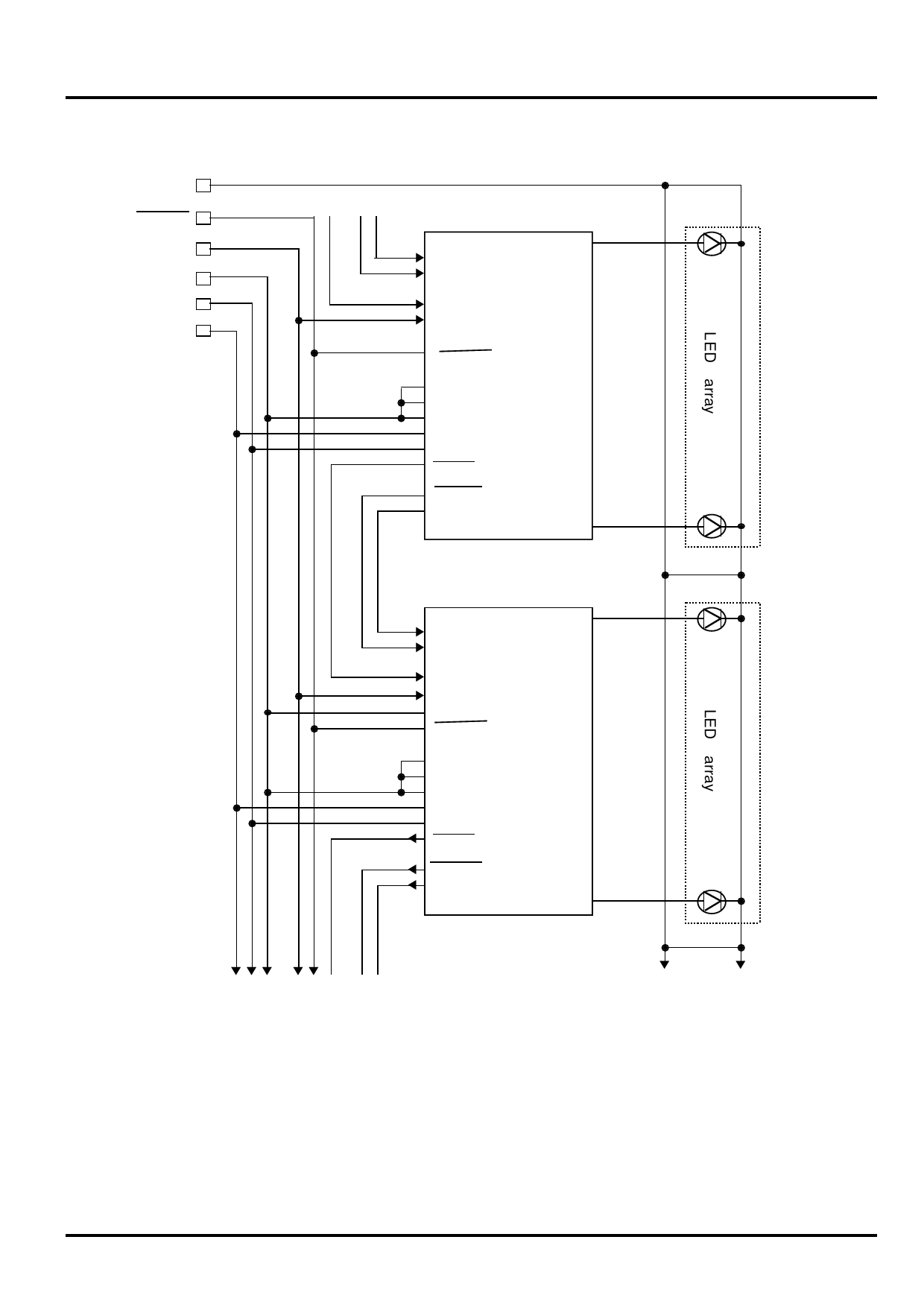
Sample Application Circuit Diagram
GND
STROBE
VREF
VSS
VDD1
VDD2
(Input signal)
SI
CL OCK1
OPEN
LOAD1
VREF
SEL
STROBE
ADJ(-)
ADJ(+)
VSS
VDD 2
VDD 1
LOAD2
CL OCK
SO
DO1
DO64
SI
CL OCK1
LOAD1
VREF
SEL
STROB
ADJ(-)
ADJ(+)
VSS
VDD 2
VDD 1
LOAD
CL OCK
SO
DO 1
DO64
(To the next input stage)
Note 1: The electric potential of the IC substrate is at VDD1.
Note 2: The number of cascade connection stages should be within 60. (10MHz)
Note 3: All VDD2 terminals should be bonded.
Note 4: Leave the SEL Terminal of the odd-numbered IC open, and connect the SEL terminal of even-numbered IC with
VSS.
Note 5: Apply the stable potential other than the VDD1 and VDD2 lines to the VREF terminal.
6585-5/11
Share Link: 