NJU3504FA1 查看數據表(PDF) - Japan Radio Corporation
零件编号
产品描述 (功能)
比赛名单
NJU3504FA1 Datasheet PDF : 60 Pages
| |||
NJU3504
The serial input or output operation starts when the LSB of the Serial Input / Output control register(PHY1) is
set to "1". In the external clock operation, the serial input or output operation waits to start until the external
clock come in.
When the serial shift register(PHY2) is set the data in advance, the data is output(transmitted) through the
SDO or the SDI(O) terminal. The SDI(O) terminal can be changed as a transmitter or a receiver in
accordance with the bit3(b3) of PHY1. The data order, MSB or LSB first, is selected by the mask option.
Serial Input Output operates as the 3-wire method using SDI(O), SCK and SDO terminals, or the 2-wire using
SDI(O) and SCK terminal.
<<The 3-wire method>>
The data synchronized with the falling edge of the SCK clock is output(transmitted) through the
SDO terminal. The data synchronized with the rising edge of the SCK clock is input(received)
through the SDI(O) terminals.
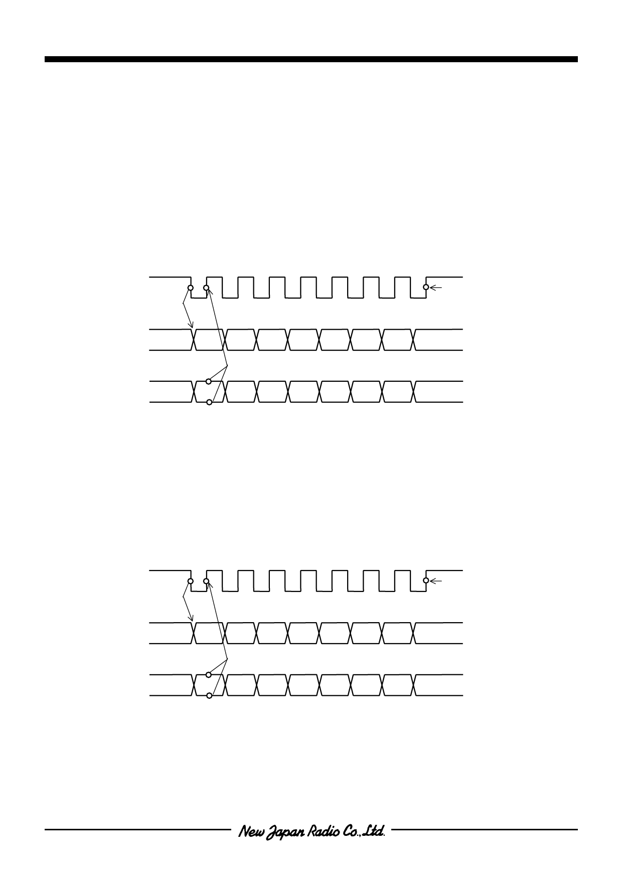
[The 3-wire transmission timing chart (MSB first)]
SCK
INTERRUPT
SIGNAL START
OUTPUT
SDO
INPUT
SDI(O)
DO7 DO6 DO5 DO4 DO3 DO2 DO1 DO0
MSB
LSB
DI7 DI6 DI5 DI4 DI3 DI2 DI1 DI0
<<The 2-wire method>>
The data synchronized with the falling edge of the SCK clock is transmitted through the SDI(O)
terminal. The data synchronized with the rising edge of the SCK clock is received through the
SDI(O) terminal.
* In case of the data transmission through the SDI(O) terminal, the SDI(O) terminal must be set as the
output by the condition of the bit3(b3) of the Serial Input / Output control register(PHY1) set to "1". In
case of the data reception through the SDI(O) terminal, the SDI(O) terminal must be set as the input by
the condition of the b3 of PHY1 set to "0".
[The 2-wire transmission timing chart (LSB first)]
SCK
INTERRUPT
SIGNAL START
OUTPUT
SDI(O)
INPUT
SDI(O)
DO0 DO1 DO2 DO3 DO4 DO5 DO6 DO7
LSB
MSB
DI0 DI1 DI2 DI3 DI4 DI5 DI6 DI7
- 31 -
Share Link: 