NJU3504FA1 查看數據表(PDF) - Japan Radio Corporation
零件编号
产品描述 (功能)
比赛名单
NJU3504FA1 Datasheet PDF : 60 Pages
| |||
NJU3504
• A/D CONTROL REGISTER {PHY7; (Y'=7)}
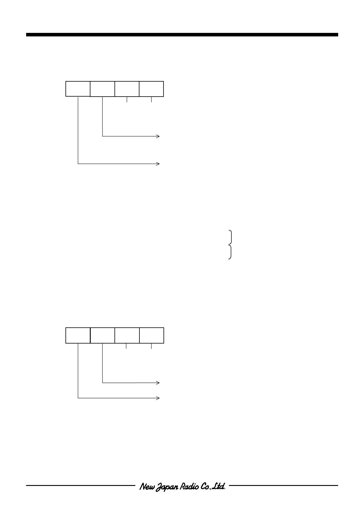
[Writing to the A/D Control Register {PHY7; (Y'=7)}]
(MSB) 3
2
1
0 (LSB)
PHY7
0
0 ⋅⋅⋅⋅⋅⋅⋅ AIN0
0
1 ⋅⋅⋅⋅⋅⋅⋅ AIN1
1
0 ⋅⋅⋅⋅⋅⋅⋅ AIN2
1
1 ⋅⋅⋅⋅⋅⋅⋅ AIN3
A/D Conversion hold mode / 1:Hold mode
Write "1" to this bit in no A/D converter operation
Start Control bit / 1:Start
EX.) An example of A/D converter start procedure for selecting AIN1 as the input and releasing the A/D hold
mode.
:
:
SRPC
LDI Y,7
LDI A,%0001
TAP
LDI A,%1001
TAP
:
:
;
;PHY7(A/D control register) is pointed
;"0001"(BIN) is stored to AC
;Data transferred from AC to PHY7
;"1001"(BIN) is stored to AC
;Data transferred from AC to PHY7
AIN1 as the input,
Releasing Hold mode
Start of conversion
REMARKS) In the external clock operation, the external clock must be input to the ADCK terminal before the start
of A/D conversion.
[Reading from the A/D Control Register]
(MSB) 3
2
1
0 (LSB)
PHY7
0
0 ⋅⋅⋅⋅⋅⋅⋅ AIN0
0
1 ⋅⋅⋅⋅⋅⋅⋅ AIN1
1
0 ⋅⋅⋅⋅⋅⋅⋅ AIN2
1
1 ⋅⋅⋅⋅⋅⋅⋅ AIN3
A/D Conversion hold mode / 1:Hold mode
End of Conversion(EOC) flag / 0:Converting, 1:END
- 41 -
Share Link: 