NLX2G66MU3TCG(2016) 查看數據表(PDF) - ON Semiconductor
零件编号
产品描述 (功能)
比赛名单
NLX2G66MU3TCG Datasheet PDF : 11 Pages
| |||
NLX2G66
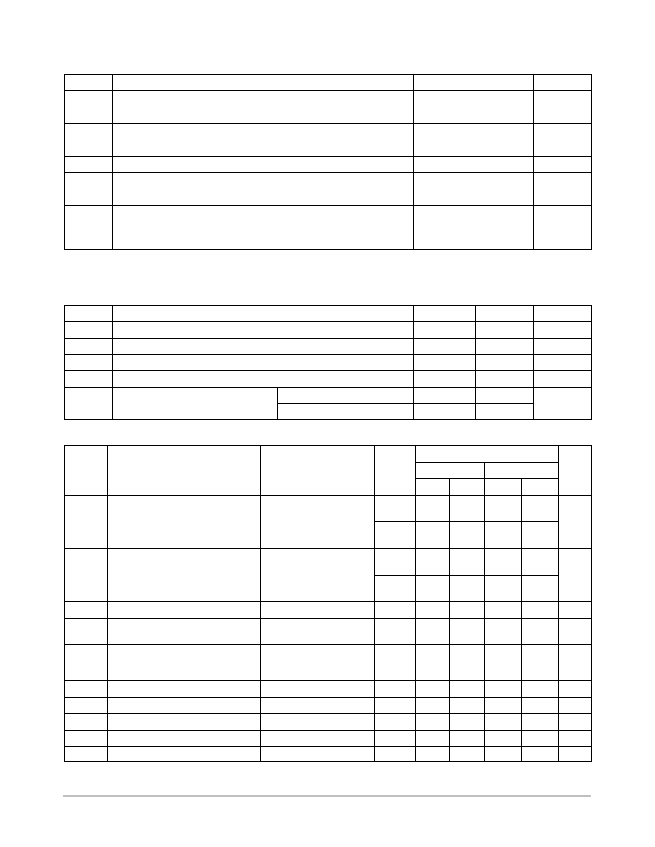
Table 1. MAXIMUM RATINGS
Symbol
Rating
Value
Unit
VCC Positive DC Supply Voltage
−0.5 to +7.0
V
VS
Switch Input / Output Voltage
(Pins 1A, 1B, 2A and 2B)
−0.5 to + VCC + 0.5
V
VI
Digital Control Input Voltage
(Pins 1C and 2C)
−0.5 to +7.0
V
IOK
I/O port diode current
±50
mA
IIK
Control input diode current
−50
mA
II/O
Continuous DC Current Through Analog Switch
±100
mA
IL
Latch−up Current, (Above VCC and below GND at 125°C)
±100
mA
Ts
Storage Temperature
−65 to +150
°C
VESD ESD Withstand Voltage:
Human Body Model (HBM)
Machine Model (MM)
≥ 5000
V
> 400
Stresses exceeding those listed in the Maximum Ratings table may damage the device. If any of these limits are exceeded, device functionality
should not be assumed, damage may occur and reliability may be affected.
Table 2. RECOMMENDED OPERATING CONDITIONS
Symbol
Parameter
Min
Max
Unit
VCC Positive DC Supply Voltage
VS
Switch Input / Output Voltage
VI
Digital Control Input Voltage
TA
Operating Temperature Range
tr, tf
Input Transition Rise or Fall Time
(ON/OFF Control Input)
(Pins 1A, 2A, 1B and 2B)
(Pins 1C and 2C)
VCC = < 3.0 V
VCC = ≥ 3.0 V
1.65
GND
GND
−55
0
0
5.5
VCC
5.5
+125
20
10
V
V
V
°C
ns/V
Table 3. ELECTRICAL CHARACTERISTICS
Symbol
VIH
Parameter
High−Level Input Voltage, Control
Input
VIL
Low−Level Input Voltage, Control
Input
II
IS(ON)
Input Leakage Current, Control Input
ON−State Switch Leakage Current
IS(OFF)
OFF−State Switch
Leakage Current
ICC
ΔICC
CI
CI/O(Off)
CI/O(On)
Quiescent Supply Current
Supply Current Change
Control Input Capacitance
Switch OFF Input / Output Capacitance
Switch ON Input / Output Capacitance
Condition
VI = VCC or GND
VIS = VCC or GND,
VI = VIH, VOS = Open
VIS = VCC and VOS =
GND, or VIS = GND and
VOS = VCC GND, VI = VIL,
VI = VCC or GND
VI = VCC – 0.6
See Figure 3
See Figure 4
VCC
1.65 to
1.95
2.3 to
5.5
1.65 to
1.95
2.3 to
5.5
5.5
5.5
5.5
5.5
5.5
5
5
5
Guaranteed Limit
255C
−555 to 1255C
Min Max Min Max
VCC x
0.65
VCC x
0.7
VCC x
0.35
VCC x
0.30
±0.1
±1
±0.1
±1
Unit
V
V
mA
mA
±0.1
±1
mA
1.0
10
mA
500
mA
3.0
pF
6.0
pF
13
pF
www.onsemi.com
2
Share Link: 