GLT6200L08LI-70FG 查看數據表(PDF) - G-Link Technology
零件编号
产品描述 (功能)
比赛名单
GLT6200L08LI-70FG Datasheet PDF : 12 Pages
| |||
G-LINK
GLT6200L08
Ultra Low Power 256k x 8 CMOS SRAM
Nov 2000(Rev. 1.0)
Features :
Description :
∗ Low-power consumption.
The GLT6200L08 is a low power CMOS Static
-active: 30mA at 55ns.
RAM organized as 262,144 x 8 bits. Easy memory
-stand by :
expansion is provided by an active LOW CE1 an
10 µA (CMOS input / output)
2 µA (CMOS input / output, SL)
active LOW OE , and Tri-state I/O’s. This device has
∗ Single +2.7 to 3.3V power supply.
∗ Equal access and cycle time.
∗ 55/70/85 ns access time.
∗ 1.0V data retention mode.
an automatic power-down mode feature when
deselected.
Writing to the device is accomplished by taking
chip Enable 1 ( CE1 ) with Write Enable ( WE ) LOW.
∗ TTL compatible, tri-state input/output. Reading from the device is performed by taking Chip
∗ Automatic power-down when deselected. Enable 1 ( CE1 ) with Output Enable ( OE ) LOW
∗ Industrial grade (-40°C ~ 85°C)
while Write Enable ( WE ) and Chip Enable 2 (CE2)
available.
is HIGH. The I/O pins are placed in a high-impedance
∗ Package available: 32-sTSOP.
state when the device is deselected : the outputs are
48Ball CSP-BGA
disabled during a write cycle.
The GLT6200L08 comes with a 1V data retention
feature and Lower Standby Power. The GLT6200L08
is available in a 32-pin sTSOP packages.
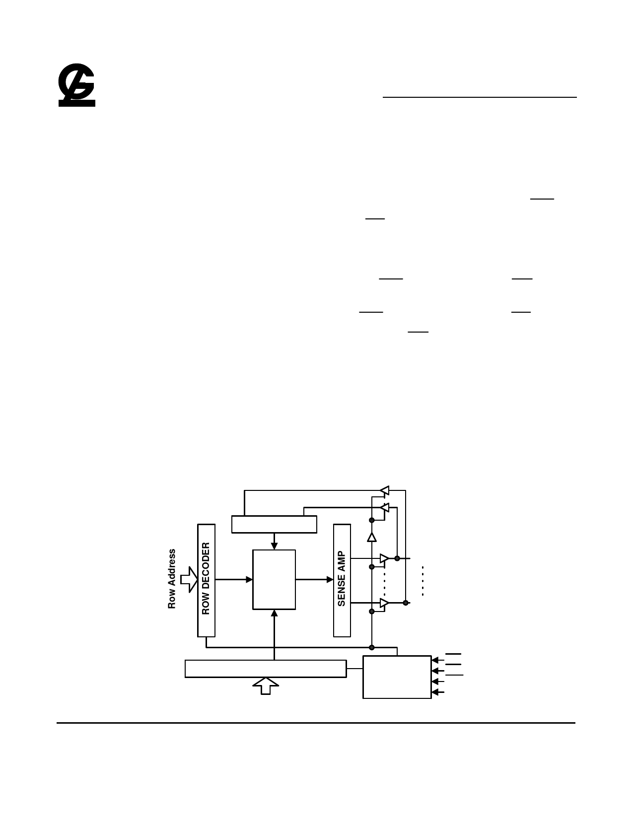
Function Block Diagram :
INPUT BUFFER
I/O7
Cell
Array
I/O1
COLUMN DECODER
G-Link Technology Corporation
2701 Northwestern Parkway
Santa Clara, CA 95051, U.S.A.
Column Address
-1-
OE
CONTROL
WE
CIRCUIT
CE1
CE2
G-Link Technology Corporation, Taiwan
6F No. 24-2, Industry E. RD. IV, Science Based
Industrial Park, Hsin Chu, Taiwan.
Share Link: 