PLL103-07 查看數據表(PDF) - PhaseLink Corporation
零件编号
产品描述 (功能)
比赛名单
PLL103-07 Datasheet PDF : 7 Pages
| |||
Preliminary PLL103-07
2 DIMM DDR Fanout Buffer
ELECTRICAL SPECIFICATIONS
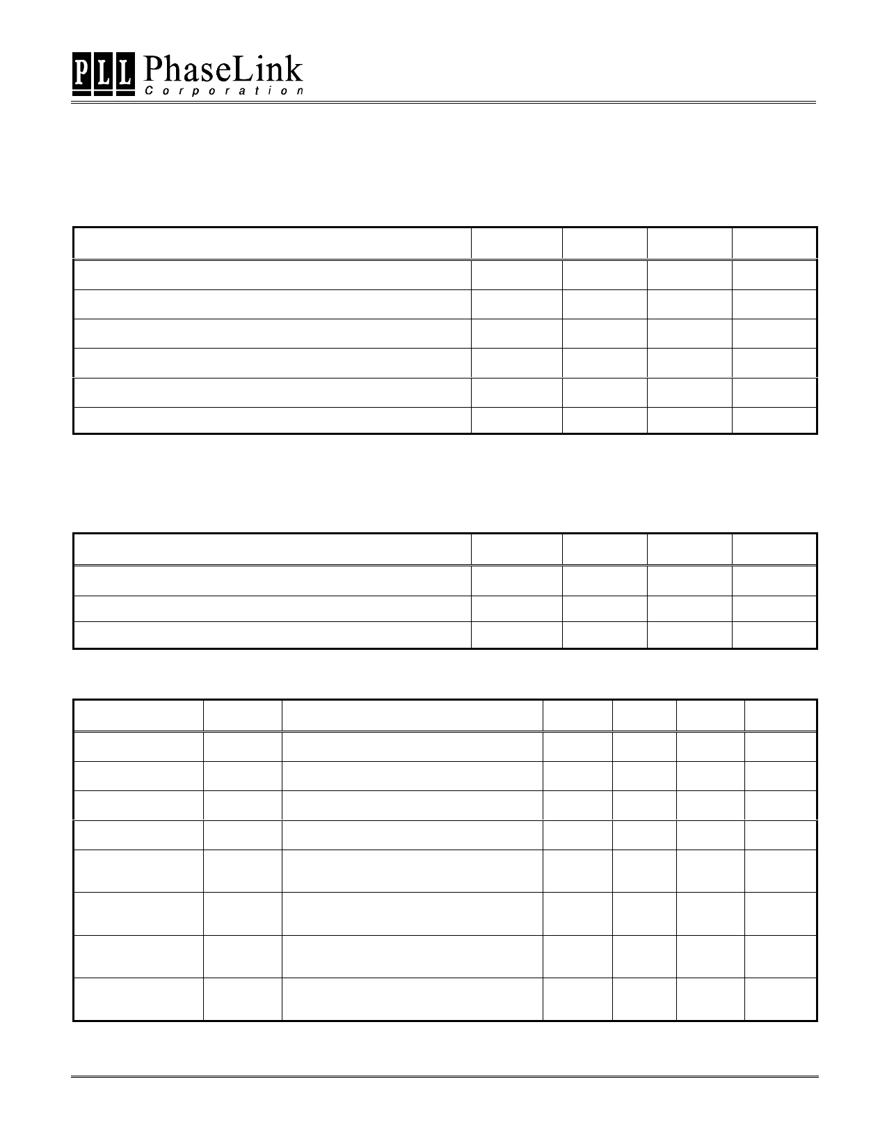
1. Absolute Maximum Ratings
PARAMETERS
SYMBOL
MIN.
MAX.
UNITS
Supply Voltage
Input Voltage, dc
Output Voltage, dc
Storage Temperature
Ambient Operating Temperature
ESD Voltage
VDD
VSS-0.5
7.0
V
VI
VSS-0.5
VDD+0.5
V
VO
VSS-0.5
VDD+0.5
V
TS
-65
150
°C
TA
0
70
°C
2
KV
Exposure of the device under conditions beyond the limits specified by Maximum Ratings for extended periods may cause permanent damage to the
device and affect product reliability. These conditions represent a stress rating only, and functional operations of the device at these or any other
conditions above the operational limits noted in this specification is not implied.
2. Operating Conditions
Supply Voltage
Input Capacitance
Output Capacitance
PARAMETERS
SYMBOL
VDD2.5
CIN
COUT
MIN.
2.375
MAX.
2.625
5
6
UNITS
V
pF
pF
3. Electrical Specifications
PARAMETERS SYMBOL
CONDITIONS
Input High Voltage
Input Low Voltage
Input High Current
Input Low Current
Output High
Voltage
Output Low
Voltage
Output High
Current
Output Low
Current
VIH
All Inputs except I2C
VIL
All inputs except I2C
IIH
VIN = VDD
IIL
VIN = 0
VOH
IOL = -12mA,
VDD = 2.375V
VOL
IOL = 12mA,
VDD = 2.375V
IOH
VDD = 2.375V, VOUT=1V
IOL
VDD = 2.375V, VOUT=1.2V
Note: TBM: To be measured
MIN.
2.0
VSS-0.3
1.7
TYP.
MAX.
VDD+0.3
0.8
TBM
TBM
UNITS
V
V
uA
uA
V
0.6
V
-18
-32
mA
26
35
mA
47745 Fremont Blvd., Fremont, California 94538 TEL (510) 492-0990 FAX (510) 492-0991
Rev 01/03/01 Page 5
Share Link: 