SSM9915K 查看數據表(PDF) - Silicon Standard Corp.
零件编号
产品描述 (功能)
比赛名单
SSM9915K Datasheet PDF : 4 Pages
| |||
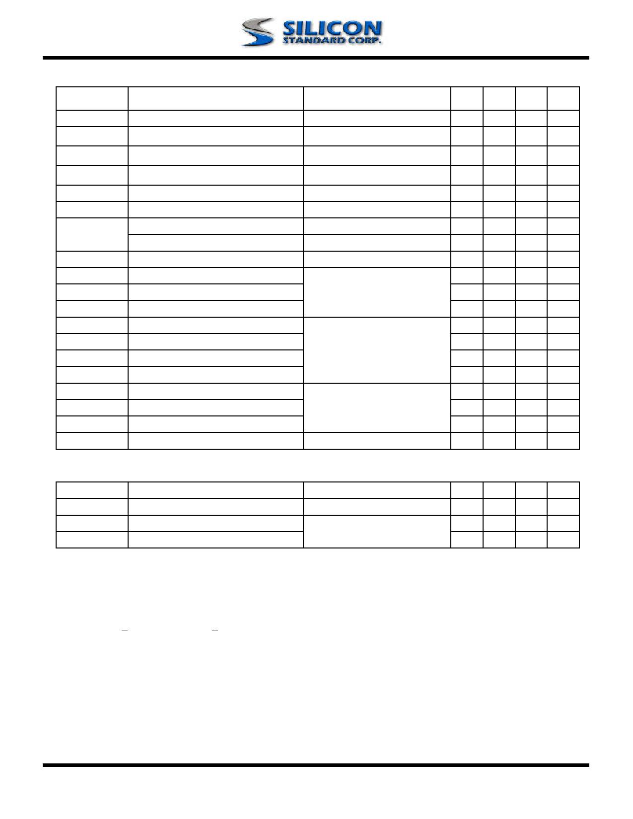
SSM9915K
Electrical Characteristics @ Tj=25oC (unless otherwise specified)
Symbol
Parameter
Test Conditions
Min. Typ. Max. Units
BVDSS
∆ BV ∆ DSS/ Tj
RDS(ON)
VGS(th)
gfs
IDSS
IGSS
Qg
Qgs
Qgd
td(on)
tr
td(off)
tf
Ciss
Coss
Crss
Rg
Drain-Source Breakdown Voltage VGS=0V, ID=250uA
Breakdown Voltage Temperature Coefficient Reference to 25°C, ID=1mA
Static Drain-Source On-Resistance2 VGS=4.5V, ID=6A
Gate Threshold Voltage
Forward Transconductance
Drain-Source Leakage Current (Tj=25oC)
Drain-Source Leakage Current (Tj=70oC)
Gate-Source Leakage
Total Gate Charge2
Gate-Source Charge
Gate-Drain ("Miller") Charge
Turn-on Delay Time2
Rise Time
Turn-off Delay Time
Fall Time
Input Capacitance
Output Capacitance
Reverse Transfer Capacitance
VGS=2.5V, ID=4A
VDS=VGS, ID=250uA
VDS=10V, ID=5A
VDS=20V, VGS=0V
VDS=16V ,VGS=0V
VGS=±12V
ID=10A
VDS=16V
VGS=4.5V
VDS=10V
ID=10A
RG=3.3Ω, VGS=5V
RD=1 Ω
VGS=0V
VDS=20V
f=1.0MHz
Gate Resistance
f=1.0MHz
20 -
-
V
- 0.03 - V/°C
-
- 50 mΩ
-
- 80 mΩ
0.5 - 1.2 V
- 13 -
S
-
-
1 uA
-
- 25 uA
-
- ±100 nA
-
5
8 nC
-
1
- nC
-
2
- nC
-
8
- ns
- 55 - ns
- 10 - ns
-
3
- ns
- 360 580 pF
- 70 - pF
- 50 - pF
- 0.78 - Ω
Source-Drain Diode
Symbol
VSD
trr
Parameter
Forward On Voltage2
Reverse Recovery Time2
Qrr
Reverse Recovery Charge
Test Conditions
IS=2.5A, VGS=0V
IS=10A, VGS=0V,
dI/dt=100A/µs
Min. Typ. Max. Units
-
- 1.3 V
- 17 - ns
-
9
- nC
Notes:
1.Pulse width limited by safe operating area.
2.Pulse width <300us , duty cycle <2%.
3.t≦10sec , Surface mounted on 1 in2 copper pad of FR4 board.
Rev.1.01 4/06/2004
www.SiliconStandard.com
2 of 4
Share Link: 