ADG728(2000) 查看數據表(PDF) - Analog Devices
零件编号
产品描述 (功能)
比赛名单
ADG728 Datasheet PDF : 12 Pages
| |||
ADG728/ADG729
TIMING CHARACTERISTICS1
(VDD = 2.7 V to 5.5 V. All specifications –40؇C to +85؇C, unless otherwise noted.)
Parameter
Limit at TMIN, TMAX
Unit
Conditions/Comments
fSCL
400
t1
2.5
t2
0.6
t3
1.3
t4
0.6
t5
100
t62
0.9
0
kHz max
ms min
ms min
ms min
ms min
ns min
ms max
ms min
SCL Clock Frequency
SCL Cycle Time
tHIGH, SCL High Time
tLOW, SCL Low Time
tHD, STA, Start/Repeated Start Condition Hold Time
tSU, DAT, Data Setup Time
tHD, DAT, Data Hold Time
t7
0.6
t8
0.6
t9
1.3
ms min
ms min
ms min
tSU, STA, Setup Time for Repeated Start
tSU, STO, Stop Condition Setup Time
tBUF, Bus Free Time Between a STOP Condition and
a Start Condition
t10
300
20 + 0.1Cb3
t11
250
300
0.1Cb3
Cb
400
tSP4
50
ns max
ns min
ns max
ns max
ns min
pF max
ns max
tR, Rise Time of Both SCL and SDA when Receiving
tF, Fall Time of SDA when Receiving
tF, Fall Time of SDA when Transmitting
Capacitive Load for Each Bus Line
Pulsewidth of Spike Suppressed
NOTES
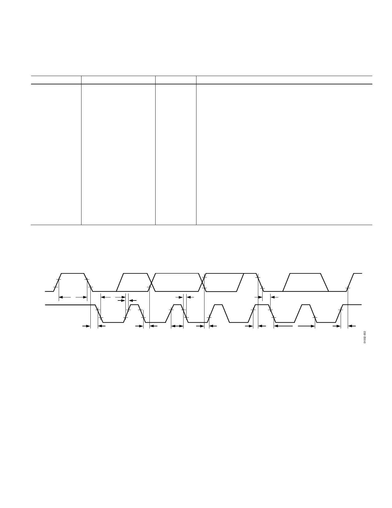
1See Figure 1.
2A master device must provide a hold time of at least 300 ns for the SDA signal (referred to the V IH min of the SCL signal) in order to bridge the undefined region of
the falling edge of SCL.
3Cb is the total capacitance of one bus line in pF. tR and tF measured between 0.3 VDD and 0.7 VDD.
4Input filtering on both the SCL and SDA inputs suppress noise spikes which are less than 50 ns.
Specifications subject to change without notice.
SDA
t9
t3
t10
t11
t4
SCL
t4
START
CONDITION
t6
t2
t5
START
CONDITION
t7
t1
REPEATED
START
CONDITION
Figure 1. 2-Wire Serial Interface Timing Diagram
t8
STOP
CONDITION
–4–
REV. A
Share Link: 