T35L6464A 查看數據表(PDF) - Taiwan Memory Technology
零件编号
产品描述 (功能)
比赛名单
T35L6464A Datasheet PDF : 16 Pages
| |||
tm TE
CH
T35L6464A
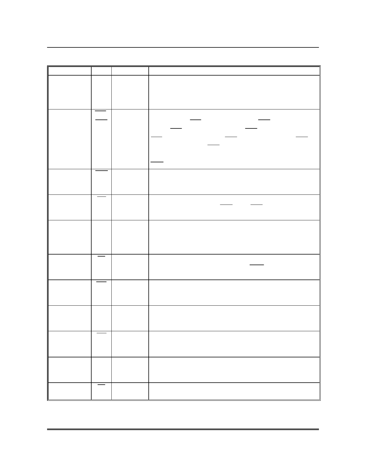
PIN DESCRIPTIONS
QFP PINS
42-44, 47-51,
53-57, 60-62
107, 108, 111,
112,117-120
114
113
115
121
124
126
125
127
116
SYM. TYPE
DESCRIPTION
A0-
Input- Addresses: These inputs are registered and must meet the setup and
A15 Synchronous hold times around the rising edge of CLK. The burst counter
generates internal addresses associated with A0 and A1,during burst
cycle and wait cycle.
BW1- Input- Byte Write: A byte write is LOW for a WRITE cyle and HIGH for
BW8 Synchronous a READ cycle. BW1 controls DQ1-DQ8. BW2 controls DQ9-
DQ16. BW3 controls DQ17-DQ24. BW4 controls DQ25-DQ32.
BW5 controls DQ33-DQ40. BW6 controls DQ41-DQ48. BW7
controls DQ49-DQ56. BW8 controls DQ57-DQ64. Data I/O are
high impedance if either of these inputs are LOW ,conditioned by
BWE being LOW.
BWE Input- Write Enable: This active LOW input gates byte write operations
Synchronous and must meet the setup and hold times around the rising edge of
CLK.
GW
Input- Global Write: This active LOW input allows a full 64-bit WRITE
Synchronous to occur independent of the BWE and BWn lines and must meet
the setup and hold times around the rising edge of CLK.
CLK Input- Clock: This signal registers the addresses, data, chip enables, write
Synchronous control and burst control inputs on its rising edge. All synchronous
inputs must meet setup and hold times around the clock's rising
edge.
CE
Input- Synchronous Chip Enable: This active LOW input is used to enable
Synchronous the device and conditions internal use of ADSP . This input is
sampled only when a new external address is loaded.
CE2 Input- Synchronous Chip Enable: This active LOW input is used to enable
Synchronous the device. This input is sampled only when a new external address
is loaded. This input can be used for memory depth expansion.
CE2 Input- Synchronous Chip Enable: This active HIGH input is used to enable
Synchronous the device. This input is sampled only when a new external address
is loaded. This input can be used for memory depth expansion.
CE3 Input- Synchronous Chip Enable: This active LOW input is used to enable
Synchronous the device. This input is sampled only when a new external address
is loaded. This input can be used for memory depth expansion.
CE3 Input- Synchronous Chip Enable: This active HIGH input is used to enable
Synchronous the device. This input is sampled only when a new external address
is loaded. This input can be used for memory depth expansion.
OE
Input Output enable: This active LOW asynchronous input enables the
data output drivers.
Taiwan Memory Technology, Inc. reserves the right P. 3
to change products or specifications without notice.
Publication Date: AUG. 1998
Revision: E
Share Link: 