QN8075 查看數據表(PDF) - Unspecified
零件编号
产品描述 (功能)
比赛名单
QN8075 Datasheet PDF : 19 Pages
| |||
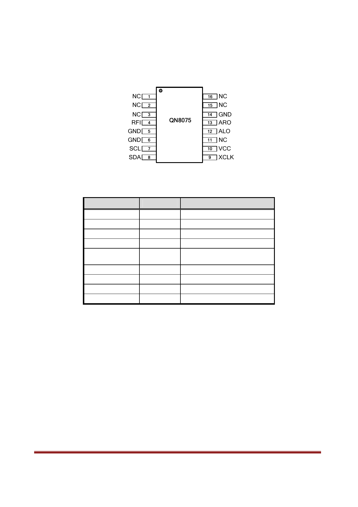
1 Pin Assignment
(Top View)
Figure 1 QN8075 Pin Out SOP16/SSOP16
Table 1: Pin Descriptions
SOP16/SSOP16
1/2/3/11/15/16
5/6/14
4
7
8
9
10
12
13
NAME
NC
GND
RFI
SCL
SDA
XCLK
VCC
ALO
ARO
DESCRIPTION
No connect
Ground
FM Receiver RF input
Clock for I2C serial bus.
Bi-directional data line for I2C serial
bus.
Clock input
Voltage supply
Analog audio output – left channel
Analog audio output – right channel
Rev 0.2c (09/02)
Copyright ©2011 by Quintic Corporation
Page 3
Confidential A
Confidential Information contained herein is covered under Non-Disclosure Agreement (NDA).
Advance Technical Information. This is a product under development. Characteristics and specifications are subject to change without notice.
Share Link: 