QN8075 查看數據表(PDF) - Unspecified
零件编号
产品描述 (功能)
比赛名单
QN8075 Datasheet PDF : 19 Pages
| |||
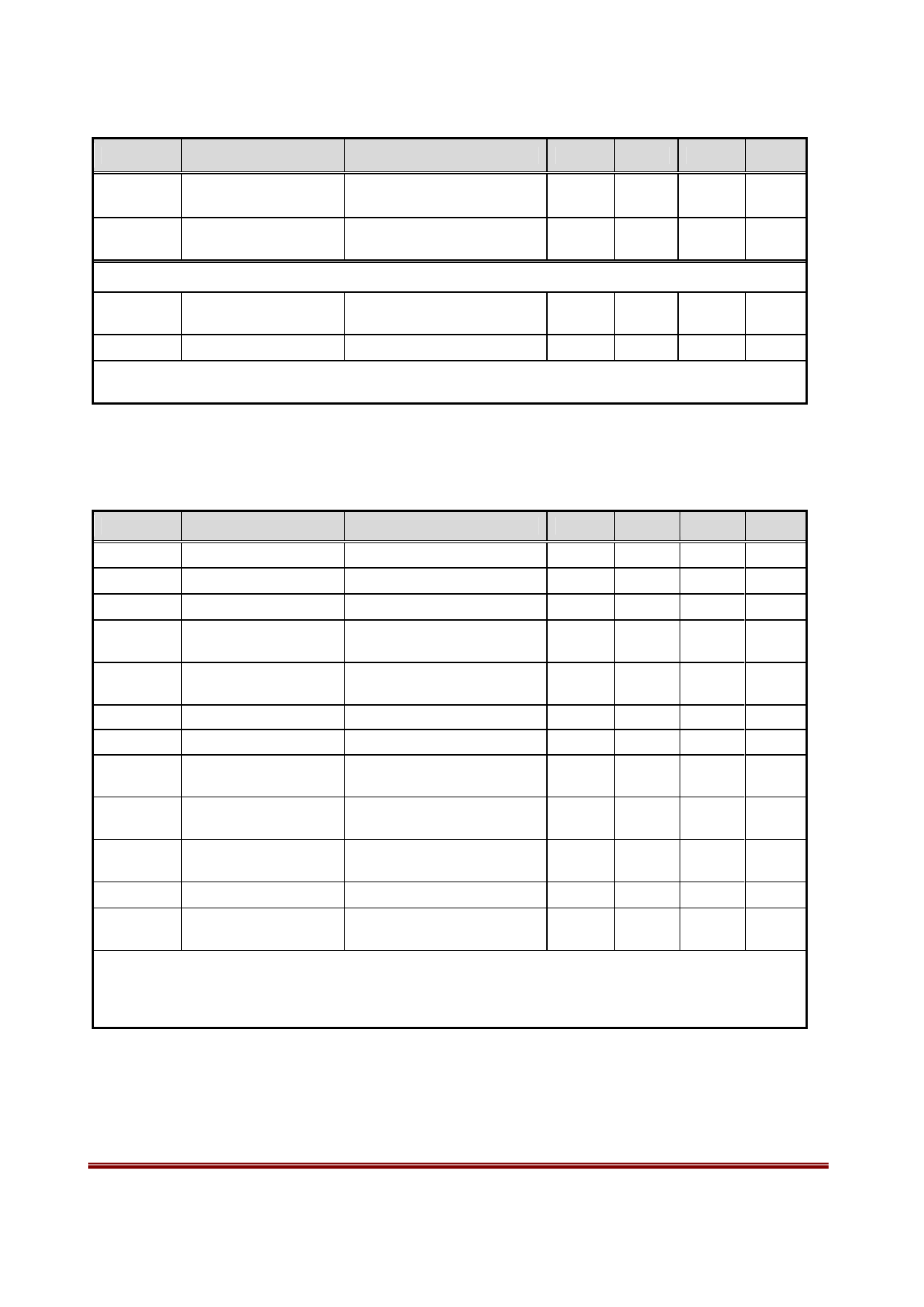
SYMBOL
PARAMETER
τpup
Chip power-up time 1
τchsw
Channel switching
time1
Receiver Timing
τwkup
Wake-up time from
standby to receive
τtune
Tune time
Notes:
1. Guaranteed by design.
CONDITIONS
From power up to register
access.
From any channel to any
channel.
Standby to RX mode.
Per channel during CCA.
MIN
TYP
MAX UNIT
20
ms
200
ms
200
ms
50
ms
Table 8: I2C Interface Timing Characteristics
(Typical values are at Vcc = 3.3V and TA = 25oC).
SYMBOL
PARAMETER
fSCL
I2C clock frequency
tLOW
Clock Low time
tHI
Clock High time
tST
SCL input to SDA
falling edge start 1,3
tSTHD
trc
tfc
tdtHD
SDA falling edge to
SCL falling edge start3
SCL rising edge3
SCL falling edge3
SCL falling edge to
next SDA rising edge3
tdtc
SDA rising edge to
next SCL rising edge3
tstp
SCL rising edge to
SDA rising edge 2,3
tw
Duration before restart3
Cb
SCL, SDA capacitive
loading3
Notes:
1. Start signaling of I2C interface.
2. Stop signaling of I2C interface.
3. Guaranteed by design.
CONDITIONS
Level from 30% to 70%
Level from 70% to 30%
MIN
1.3
0.6
0.8
0.8
20
0.6
1.3
TYP
MAX
400
UNIT
kHz
μs
μs
μs
μs
300
ns
300
ns
ns
900
ns
μs
μs
10
pF
Rev 0.2c (09/02)
Copyright ©2011 by Quintic Corporation
Page 7
Confidential A
Confidential Information contained herein is covered under Non-Disclosure Agreement (NDA).
Advance Technical Information. This is a product under development. Characteristics and specifications are subject to change without notice.
Share Link: 