QN8075 查看數據表(PDF) - Unspecified
零件编号
产品描述 (功能)
比赛名单
QN8075 Datasheet PDF : 19 Pages
| |||
2 Electrical Specifications
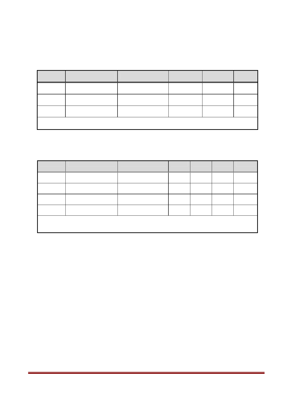
Table 2: Absolute Maximum Ratings
SYMBOL
PARAMETER
CONDITIONS
Vbat
Supply voltage
VCC to GND
VIO1
Logic signal level
SCL, SDA to GND
Ts
Storage temperature
Notes:
1. VIO is pulled up externally via resisters.
MIN
-0.3
-0.3
-55
MAX
5
3.6
+150
UNIT
V
V
oC
Table 3: Recommended Operating Conditions
SYMBOL
PARAMETER
CONDITIONS
Vcc
Supply voltage
VCC to GND
TA
Operating temperature
RFin
RF input level1
Peak input voltage
VIO2
Digital I/O voltage
Notes:
1. At RF input pin, RFI.
2. VIO is pulled up externally via resisters.
MIN
2.7
-25
1.6
TYP
3.3
MAX
5.0
+85
0.3
3.6
UNIT
V
oC
V
V
Rev 0.2c (09/02)
Copyright ©2011 by Quintic Corporation
Page 4
Confidential A
Confidential Information contained herein is covered under Non-Disclosure Agreement (NDA).
Advance Technical Information. This is a product under development. Characteristics and specifications are subject to change without notice.
Share Link: 