CMX631A 查看數據表(PDF) - CML Microcircuits
零件编号
产品描述 (功能)
比赛名单
CMX631A Datasheet PDF : 16 Pages
| |||
Low Voltage SPM Detector
CMX631A
4.3.2 Input Gain Components
Refer to the gain components found in Table 2 and Figure 2. The user should calculate and select external
components (R1/R2/C3 and R3/R4/C4) to provide amplifier gain within the limits obtained in 4.3.1 Input Gain
Calculation.
Component tolerances should not move the gain-figure outside these limits. The graphs Figure 4 and Figure 5 are
for the calculation of input gain components for a CMX631A using a VDD of 3.0 (±0.1) or VDD of 5.0 (±0.5).
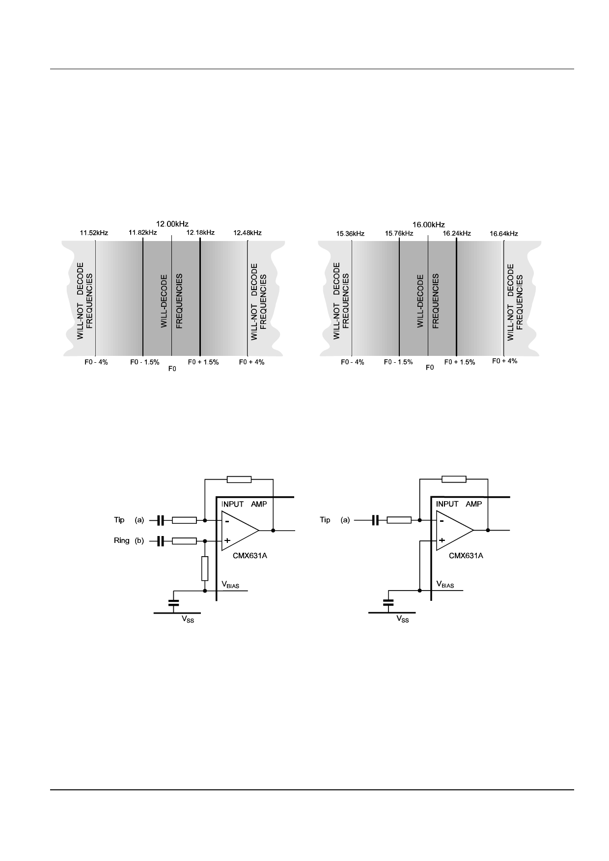
4.4 ‘WILL’/’WILL-NOT’ Detect Frequencies
Figure 6: ‘WILL’/’WILL-NOT’ Detect Frequencies
5 Applications
5.1 Input Configurations
Figure 7: Input Configurations
5.1.1 Protection Against High Voltages
Telephone systems may have high DC and AC voltages present on the line. If the CMX631A is a part of host
equipment that has its own signal input protection circuitry, there will be no need for further protection as long as the
voltage on any pin is limited to within VDD +0.3V and VSS -0.3V.
If the host system does not have input protection, or there are signals present outside the device's specified limits,
the CMX631A will require protection diodes at its signal inputs (+ and -). The breakdown voltage of the capacitors
and the peak inverse voltage of the diodes must be sufficient to withstand the sum of the DC voltages plus all
expected signal peaks.
© 1998 Consumer Microcircuits Limited
9
D/631A/1
Share Link: 