74ABT899 查看數據表(PDF) - Fairchild Semiconductor
零件编号
产品描述 (功能)
比赛名单
74ABT899 Datasheet PDF : 16 Pages
| |||
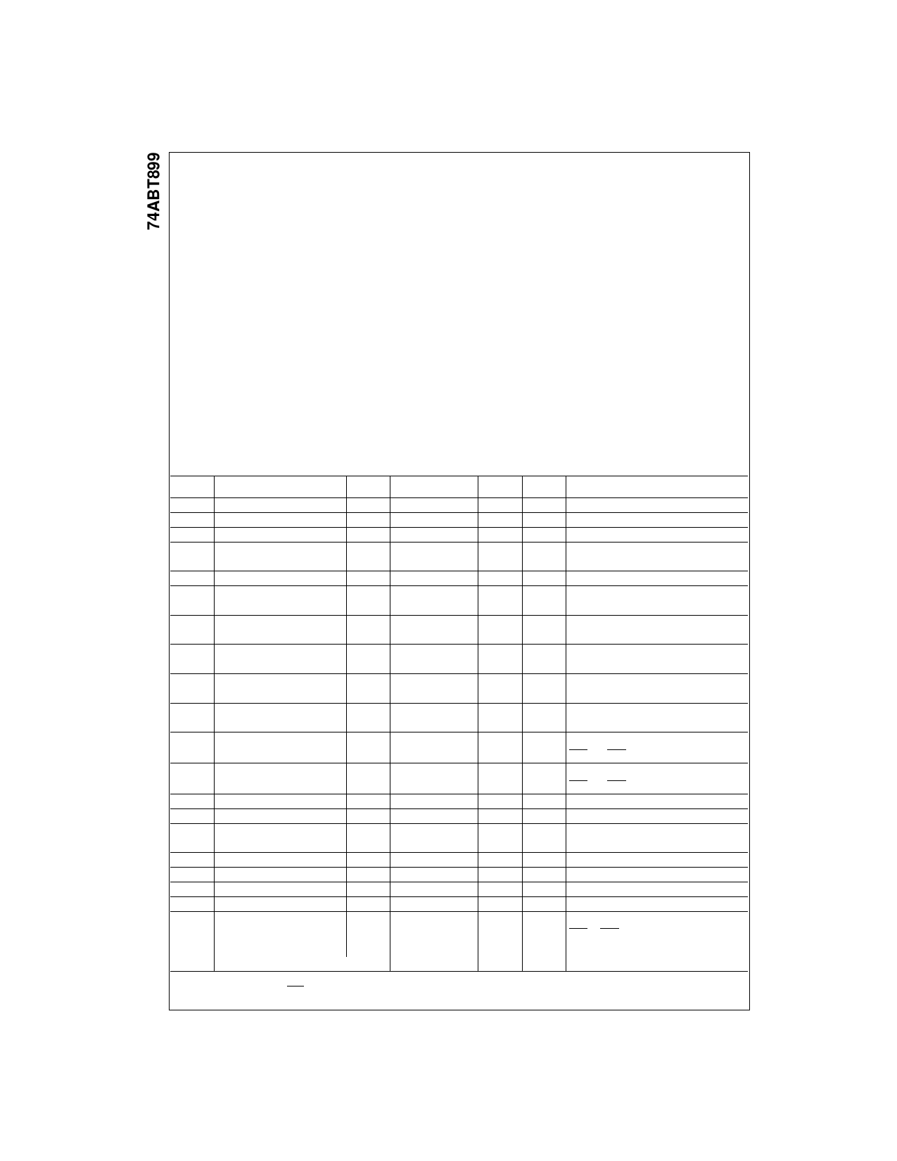
Absolute Maximum Ratings(Note 2)
Storage Temperature
Ambient Temperature under Bias
Junction Temperature under Bias
Plastic
VCC Pin Potential to
Ground Pin
Input Voltage (Note 3)
Input Current (Note 3)
Voltage Applied to Any Output
in the Disable or Power-
Off State
in the HIGH State
Current Applied to Output
in LOW State (Max)
−65°C to +150°C
−55°C to +125°C
−55°C to +150°C
−0.5V to +7.0V
−0.5V to +7.0V
−30 mA to +5.0 mA
−0.5V to +5.5V
−0.5V to VCC
twice the rated IOL (mA)
DC Latchup Source Current
Over Voltage Latchup (I/O)
−500 mA
10V
Recommended Operating
Conditions
Free Air Ambient Temperature
−40°C to +85°C
Supply Voltage
+4.5V to +5.5V
Minimum Input Edge Rate (∆V/∆t)
Data Input
50 mV/ns
Enable Input
20 mV/ns
Note 2: Absolute maximum ratings are values beyond which the device
may be damaged or have its useful life impaired. Functional operation
under these conditions is not implied.
Note 3: Either voltage limit or current limit is sufficient to protect inputs.
DC Electrical Characteristics
Symbol
Parameter
VIH
Input HIGH Voltage
VIL
Input LOW Voltage
VCD
Input Clamp Diode Voltage
VOH
Output HIGH
Voltage
VOL
Output LOW Voltage
VID
Input Leakage Test
Min
Typ
2.0
2.5
2.0
4.75
IIH
Input HIGH Current
IBVI
IBVIT
IIL
Input HIGH Current
Breakdown Test
Input HIGH Current
Breakdown Test (I/O)
Input LOW Current
IIH + IOZH Output Leakage Current
IIL + IOZL Output Leakage Current
IOS
ICEX
IZZ
Output Short-Circuit Current
Output HIGH Leakage Current
Bus Drainage Test
−100
ICCH
ICCL
ICCZ
ICCT
ICCD
Power Supply Current
Power Supply Current
Power Supply Current
Additional ICC/Input
Dynamic ICC: No Load
(Note 4)
Note 4: Guaranteed, but not tested.
Note 5: Add 3.75 mA for each ERR LOW.
Max
Units
VCC
Conditions
V
Recognized HIGH Signal
0.8
V
Recognized LOW Signal
−1.2
V
V
0.55
V
V
Min IIN = −18 mA (Non I/O Pins)
Min IOH = −3 mA, (An, Bn, APAR, BPAR)
IOH = −32 mA, (An, Bn, APAR, BPAR)
Min IOL = 64 mA, (An, Bn, APAR, BPAR)
0.0 IID = 1.9 µA, (Non-I/O Pins)
All Other Pins Grounded
5
µA
Max VIN = 2.7V (Non-I/O Pins) (Note 4)
VIN = VCC (Non-I/O Pins)
7
µA
Max VIN = 7.0V (Non-I/O Pins)
100
µA
Max VIN = 5.5V (An, Bn, APAR, BPAR)
−5
50
−50
−275
50
100
250
34
250
2.5
0.4
µA
Max VIN = 0.5V (Non-I/O Pins) (Note 4)
VIN = 0.0V (Non-I/O Pins)
µA
0V–5.5V VOUT = 2.7V (An, Bn);
GAB and GBA = 2.0V
µA
0V–5.5V VOUT = 0.5V (An, Bn);
GAB and GBA = 2.0V
mA
Max VOUT = 0V (An, Bn, APAR, BPAR)
µA
Max VOUT = VCC (An, Bn, APAR, BPAR)
µA
0.0V VOUT = 5.5V (An, Bn, APAR, BPAR);
All Others GND
µA
mA
µA
mA
mA/MHz
Max All Outputs HIGH
Max All Outputs LOW, ERRA/B = HIGH (Note 5)
Max Outputs 3-STATE All Others at VCC or GND
Max VI = VCC − 2.1V All Others at VCC or GND
Max Outputs Open
GAB or GBA = GND, LE = HIGH
Non-I/O = GND or VCC
One bit toggling, 50% duty cycle
www.fairchildsemi.com
4
Share Link: 