ISL8510 查看數據表(PDF) - Renesas Electronics
零件编号
产品描述 (功能)
比赛名单
ISL8510 Datasheet PDF : 21 Pages
| |||
ISL8510
operation, select bulk capacitors with voltage and current
ratings above the maximum input voltage and largest RMS
current required by the circuit. Their voltage rating should be at
least 1.25x greater than the maximum input voltage, while a
voltage rating of 1.5x is a conservative guideline. For most
cases, the RMS current rating requirement for the input
capacitor of a buck regulator is approximately 1/2 the DC load
current.
The maximum RMS current required by the regulator may be
closely approximated through Equation 7:
IRMSMAX =
V---V--O--I--UN---T-
I O
U
2
TMAX
+
1--1--2--
-V----I-N--L---–-----V--f--Os----U---T-
-V--V--O--I--UN---T-
2
(EQ. 7)
For a through hole design, several electrolytic capacitors may
be needed. For surface mount designs, solid tantalum
capacitors can be used, but caution must be exercised with
regard to the capacitor surge current rating. These capacitors
must be capable of handling the surge-current at power-up.
Some capacitor series available from reputable manufacturers
are surge current tested.
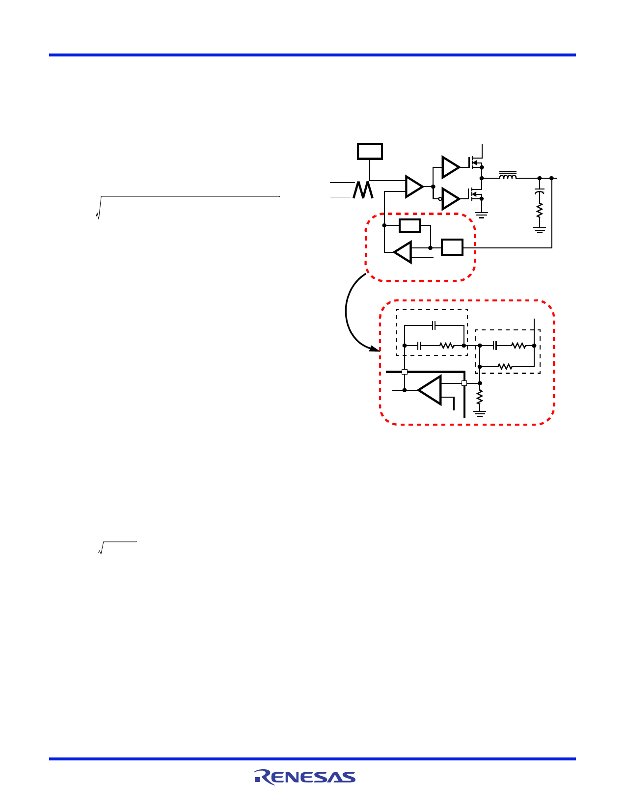
Feedback Compensation
Figure 30 highlights the voltage-mode control loop for a
synchronous-rectified buck converter. The output voltage
(VOUT) is regulated to the Reference voltage level. The error
amplifier output (VE/A) is compared with the oscillator (OSC)
triangular wave to provide a pulse-width modulated (PWM)
wave with an amplitude of VIN at the PHASE node. The PWM
wave is smoothed by the output filter (LO and CO).
The modulator transfer function is the small-signal transfer
function of VOUT/VE/A. This function is dominated by a DC
Gain and the output filter (LO and CO), with a double pole
break frequency at fLC and a zero at fESR. The DC Gain of the
modulator is simply the input voltage (VIN) divided by the peak-
to-peak oscillator voltage VOSC.
Modulator Break Frequency Equations
FLC=
---------------------1---------------------
2 x LO x CO
(EQ. 8)
FESR= 2----------x-----E----S--1---R------x-----C-----O---
(EQ. 9)
The compensation network consists of the error amplifier
(internal to the ISL6537) and the impedance networks ZIN and
ZFB. The goal of the compensation network is to provide a
closed loop transfer function with the highest 0dB crossing
frequency (f0dB) and adequate phase margin. Phase margin is
the difference between the closed loop phase at f0dB and 180°.
Equations 10 through 13 relate the compensation network’s
poles, zeros and gain to the components (R1, R2, R3, C1, C2,
and C3) in Figure 31. Use these guidelines for locating the
poles and zeros of the compensation network:
1. Pick Gain (R2/R1) for desired converter bandwidth.
2. Place 1st Zero Below Filter’s Double Pole (~75% fLC).
3. Place 2nd Zero at Filter’s Double Pole.
4. Place 1st Pole at the ESR Zero.
5. Place 2nd Pole at Half the Switching Frequency.
6. Check Gain against Error Amplifier’s Open-Loop Gain.
7. Estimate Phase Margin - Repeat if Necessary.
VOSC
OSC
PWM
COMPARATOR
+-
DRIVER
DRIVER
VIN
LO
PHASE CO
VDDQ
ZFB
VE/A
+-
ZIN
ERROR REFERENCE
AMP
ESR
(PARASITIC)
DETAILED COMPENSATION COMPONENTS
C1
C2
R2
ZFB
VDDQ
ZIN
C3 R3
COMP
R1
-
FB
+
R4
ISL8510
REFERENCE
VDDQ
=
0.8
1
+
RR-----14-
FIGURE 30. VOLTAGE-MODE BUCK CONVERTER
COMPENSATION DESIGN AND OUTPUT
VOLTAGE SELECTION
Compensation Break Frequency Equations
fZ1 = -2---------x-----R--1--2-----x------C----2-
(EQ. 10)
fZ2 = 2----------x-------R-----1----+-1----R-----3-------x-----C-----3-
fP1
=
---------------------------1-----------------------------
2
x
R2
x
C-C----11-----+x-----CC----2-2-
(EQ. 11)
(EQ. 12)
fP2 = -2---------x-----R--1--3-----x------C----3--
(EQ. 13)
Figure 31 shows an asymptotic plot of the DC/DC converter’s
gain vs frequency. The actual Modulator Gain has a high gain
peak due to the high Q factor of the output filter and is not
shown in Figure 31. Using the guidelines from “Modulator
Break Frequency Equations” on page 18 should give a
Compensation Gain similar to the curve plotted. The open loop
error amplifier gain bounds the compensation gain. Check the
compensation gain at fP2 with the capabilities of the error
FN6516 Rev 2.00
December 15, 2008
Page 18 of 21
Share Link: 