LC86E4332 查看數據表(PDF) - SANYO -> Panasonic
零件编号
产品描述 (功能)
比赛名单
LC86E4332 Datasheet PDF : 19 Pages
| |||
LC86E4332
Pin Description
• Port option can be specified by bit units.
• At port 0, 'Pull-up resistor provided' when specifying CMOS output.
'Pull-up resistor not provided' when specifying N-ch open drain output.
• At port 1, 'Programmable pull-up resistor provided' when specifying either CMOS or N-ch open drain output.
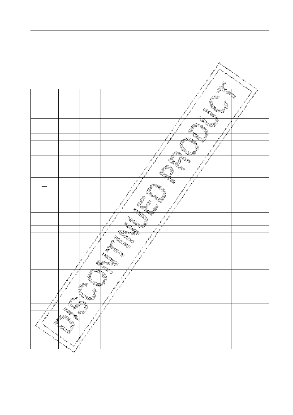
Pin Description Table
Pin name Pin No.
I/O
Function description
Option
PROM mode
DVSS
9
—
Negative power supply for digital circuit
CF1
10
I
Input terminal for ceramic resonator
CF2
11
O
Output terminal for ceramic resonator
DVDD
12
—
Positive power supply for digital circuit
RES
17
I
Reset terminal
LC1
18
I
LC oscillation circuit input terminal
LC2
19
O
LC oscillation circuit output terminal
FILT
20
O
Filter terminal for PLL
AVDD
21
—
Positive power supply for analog circuit
AVSS
22
—
Negative power supply for analog circuit
CVIN
23
I
Video signal input terminal
VS
24
I
Vertical synchronization signal input terminal
HS
25
I
Horizontal synchronization signal input
terminal
I
26
O
Image intensity output
R
27
O
Red (R) output terminal of RGB image output
A4 (*1)
G
28
O
Green (G) output terminal of RGB image
output
A5 (*1)
B
29
O
Blue (B) output terminal of RGB image output
A6 (*1)
BL
30
O
Fast blanking control signal
Switch TV image signal and caption/OSD
image signal
A7 (*1)
PWM0
31 to 40
O
PWM0 to 9 output terminal
to PWM9
15 V withstand
PWM0 to 8 :
A8 to A16 (*1)
PWM9 : "L" fixed
Port 0
8-bit Input/output port
Pull-up resistor
P00 to P07 45 to 52
I/O
Input/output can be specified in nibble units
Provided/not provided
HOLD release input
(in bit units)
Interrupt input
Output Format
CMOS/Nch-OD
(in bit units)
Port 1
P10 to P17
1 to 8
8-bit Input/output port
I/O
Input/output can be specified in bit units.
Other function
Output Format
CMOS/Nch-OD
(in bit units)
D0 to D7 (*2)
P10 SIO0 data output
P11 SIO0 data input /bus input/output
P12 SIO0 clock input/output
P17 Timer 1 (PWM) output
No. 5600-6/19
Share Link: 