LC86E4332 查看數據表(PDF) - SANYO -> Panasonic
零件编号
产品描述 (功能)
比赛名单
LC86E4332 Datasheet PDF : 19 Pages
| |||
LC86E4332
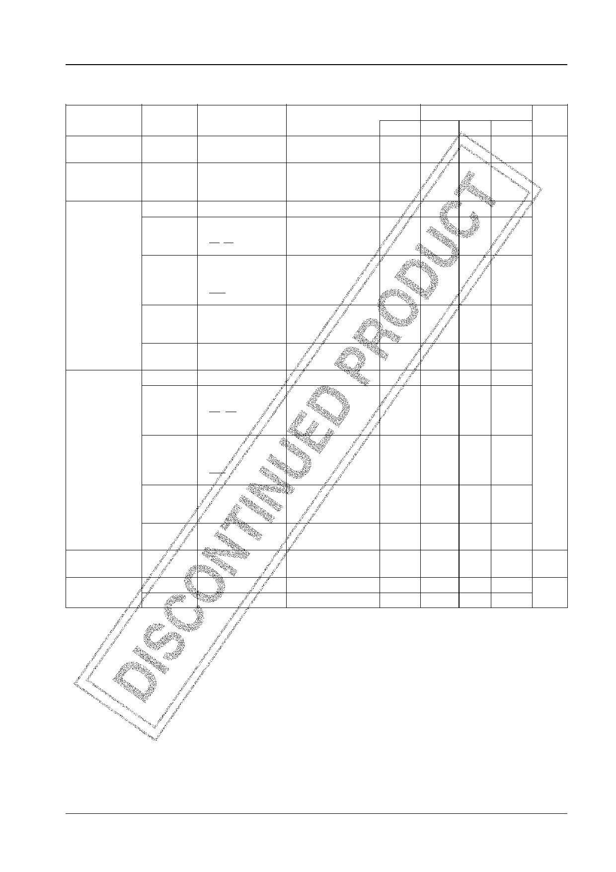
2. Recommended Operating Range at Ta = +10°C to +40°C, VSS = 0 V
Parameter
Operating supply
voltage range
Hold voltage
Input high-level
voltage
Input low-level
voltage
CVIN input
amplitude
Operation cycle
time
Symbol
VDD
VHD
VIH(1)
VIH(2)
VIH(3)
VIH(4)
VIH(5)
VIL(1)
VIL(2)
VIL(3)
VIL(4)
VIL(5)
VCVIN
tCYC(1)
tCYC(2)
Pins
Conditions
Ratings
Unit
VDD [V] min
typ
max
DVDD, AVDD
0.97 µs ≤ tCYC
tCYC ≤ 1.02 µs
4.5
5.5 V
DVDD, AVDD
RAMs and the
registers hold data
at HOLD mode.
2.0
5.5
Port 0 (Schmitt)
Output disable
4.5 to 5.5 0.6VDD
VDD
• Port 1 (Schmitt)
Output disable
4.5 to 5.5 0.75VDD
VDD
• P72, 73
• HS, VS
• P70
Output N-channel
4.5 to 5.5 0.75VDD
VDD
port input / interrupt transistor OFF
• P71
• RES
(Schmitt)
• P70
Output N-channel
4.5 to 5.5 VDD–0.5
VDD
Watchdog timer
transistor OFF
input
Port 9
port input
4.5 to 5.5 0.7VDD
VDD
Port 0 (Schmitt) Output disable
4.5 to 5.5
VSS
0.2VDD
• Port 1
• P72, 73
• HS, VS
• Port 9
(Schmitt)
Output disable
4.5 to 5.5
VSS
0.25VDD
• P70
N-channel transistor 4.5 to 5.5
VSS
port input / interrupt OFF
• P71
• RES
(Schmitt)
0.25VDD
• P70
N-channel transistor 4.5 to 5.5
VSS
Watchdog timer
OFF
input
0.6VDD
Port 9
port input
CVIN
4.5 to 5.5
VSS
5.0
1Vp-p 1Vp-p
–3dB
0.3VDD
*
1Vp-p Vp-p
+3dB
OSD function
4.5 to 5.5 0.97 1
1.02 µs
Except OSD function 4.5 to 5.5 0.97
40
* Vp-p : Peak-to-peak voltage
No. 5600-9/19
Share Link: 