UT62L64CSCL-70 查看數據表(PDF) - Utron Technology Inc
零件编号
产品描述 (功能)
比赛名单
UT62L64CSCL-70 Datasheet PDF : 12 Pages
| |||
UTRON
Rev. 1.3
UT62L64C
8K X 8 BIT LOW POWER CMOS SRAM
Notes :
1. WE , CE must be high or CE2 must be low during all address transitions.
2.A write occurs during the overlap of a low CE , high CE2, low WE .
3.During a WE controlled write cycle with OE low, tWP must be greater than tWHZ+tDW to allow the drivers to turn off and data to
be placed on the bus.
4.During this period, I/O pins are in the output state, and input signals must not be applied.
5.If the CE low transition and CE2 high transition occurs simultaneously with or after WE low transition, the outputs remain in a
high impedance state.
6.tOW and tWHZ are specified with CL = 5pF. Transition is measured ± 500mV from steady state.
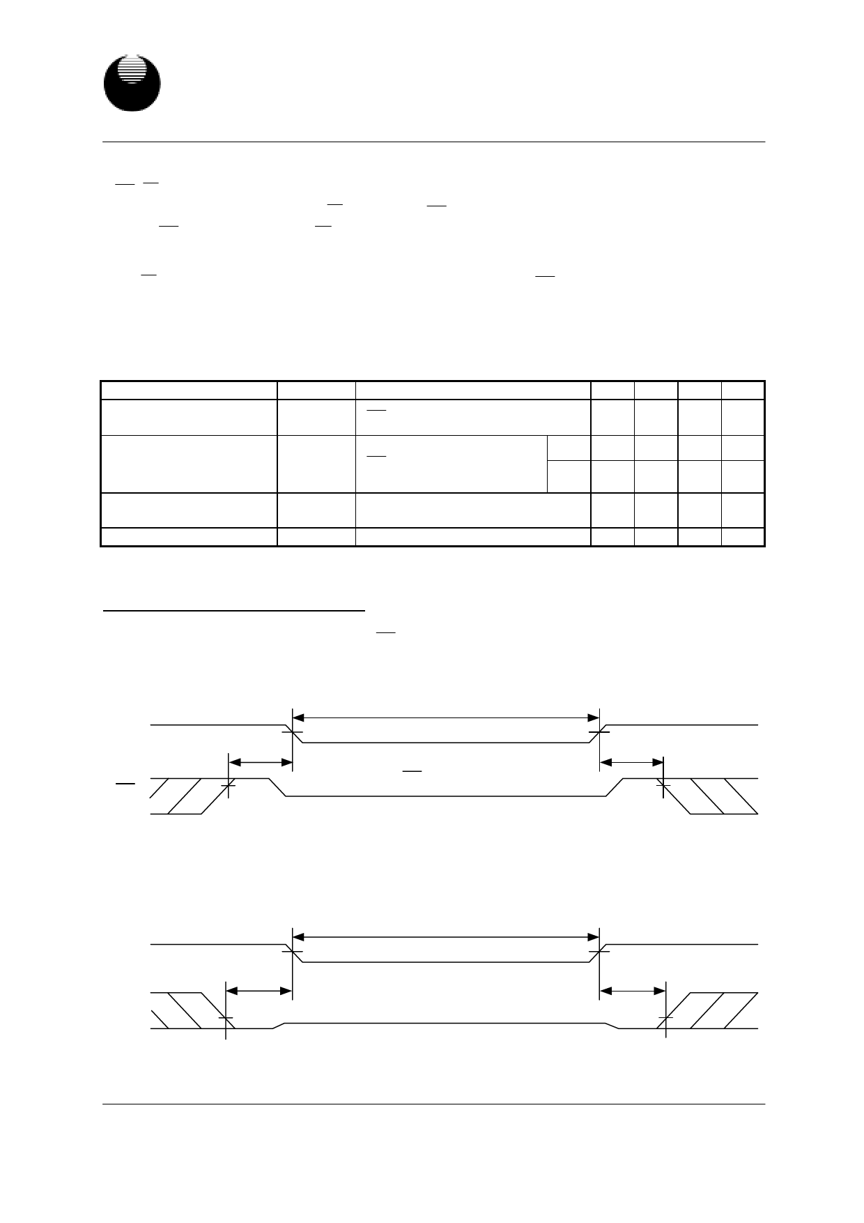
DATA RETENTION CHARACTERISTICS (TA = 0℃ to 70℃ / -20℃ to 85℃(E))
PARAMETER
Vcc for Data Retention
Data Retention Current
Chip Disable to Data
Retention Time
Recovery Time
tRC* = Read Cycle Time
SYMBOL
VDR
IDR
tCDR
tR
TEST CONDITION
CE ≧ VCC-0.2V or CE2 ≤ 0.2V
Vcc=2.5V
-L
CE ≧ VCC-0.2V
or CE2 ≤ 0.2V
-LL
See Data Retention Waveforms
(below)
MIN. TYP. MAX. UNIT
1.5 - 3.6 V
-
1 50 µA
- 0.5 10 µA
0-
tRC*
-
- ns
- ns
DATA RETENTION WAVEFORM
Low Vcc Data Retention Waveform (1) ( CE controlled)
VCC
CE
Vcc(min.)
tCDR
VIH
VDR ≧ 1.5V
CE ≧ VCC-0.2V
Vcc(min.)
tR
VIH
Low Vcc Data Retention Waveform (2) (CE2 controlled)
VCC
CE2
VCC(min.)
tCDR
VIL
VDR ≧ 1.5V
CE2 ≦ 0.2V
VCC(min.)
tR
VIL
UTRON TECHNOLOGY INC.
1F, No. 11, R&D Rd. II, Science-Based Industrial Park, Hsinchu, Taiwan, R. O. C.
TEL: 886-3-5777882 FAX: 886-3-5777919
7
P80060
Share Link: 