FAN5234 查看數據表(PDF) - Fairchild Semiconductor
零件编号
产品描述 (功能)
比赛名单
FAN5234 Datasheet PDF : 15 Pages
| |||
PRODUCT SPECIFICATION
FAN5234
The voltage at the positive input of the error amplifier is lim-
ited by the voltage at the SS pin which is charged with a
5mA current source. Once CSS has charged to VREF (0.9V)
the output voltage will be in regulation. The time it takes SS
to reach 0.9V is:
T0.9
=
0----.-9-----×----C-----S---S
5
(1)
where T0.9 is in seconds if CSS is in µF.
When SS reaches 1.5V, the Power Good outputs are enabled
and hysteretic mode is allowed. The converter is forced into
PWM mode during soft start.
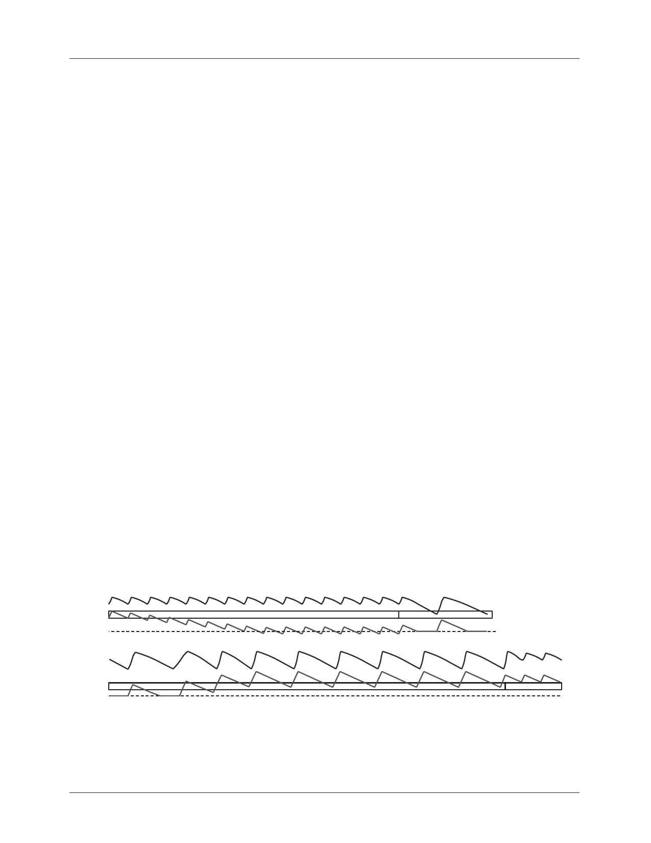
Operation Mode Control
The mode-control circuit changes the converter’s mode of
operation from PWM to Hysteretic and visa versa, based
on the voltage polarity of the SW node when the lower
MOSFET is conducting and just before the upper MOSFET
turns on. For continuous inductor current, the SW node is
negative when the lower MOSFET is conducting and the
converters operate in fixed-frequency PWM mode as shown
in Figure 3. This mode of operation achieves high efficiency
at nominal load. When the load current decreases to the point
where the inductor current flows through the lower MOSFET
in the ‘reverse’ direction, the SW node becomes positive,
and the mode is changed to hysteretic, which achieves higher
efficiency at low currents by decreasing the effective switch-
ing frequency.
To prevent accidental mode change or "mode chatter" the
transition from PWM to Hysteretic mode occurs when the
SW node is positive for eight consecutive clock cycles
(see Figure 3). The polarity of the SW node is sampled at the
end of the lower MOSFET's conduction time. At the transi-
tion between PWM and hysteretic mode both the upper and
lower MOSFETs are turned off. The SW node will ‘ring’
based on the output inductor and the parasitic capacitance on
the SW node and settle out at the value of the output voltage.
The boundary value of inductor current, where current
becomes discontinuous, can be estimated by the following
expression.
ILOAD(DIS)
=
(---V----I--N-----–-----V----O----U----T---)--V-----O----U----T-
2FSWLOUTVIN
(2)
Hysteretic Mode
Conversely, the transition from Hysteretic mode to PWM
mode occurs when the SW node is negative for 8 consecutive
cycles.
A sudden increase in the output current will also cause a
change from hysteretic to PWM mode. This load increase
causes an instantaneous decrease in the output voltage due to
the voltage drop on the output capacitor ESR. If the load
causes the output voltage (as presented at VSEN) to drop
below the hysteretic regulation level (20mV below VREF),
the mode is changed to PWM on the next clock cycle.
In hysteretic mode, the PWM comparator and the error
amplifier that provide control in PWM mode are inhibited
and the hysteretic comparator is activated. In hysteretic
mode the low side MOSFET is operated as a synchronous
rectifier, where the voltage across (VDS(ON)) it is monitored,
and it is switched off when VDS(ON) goes positive (current
flowing back from the load) allowing the diode to block
reverse conduction.
VCORE
IL
0
VCORE
IL 0
6
PWM Mode
12345678
Hysteretic Mode
Hysteretic Mode
1
2
3
4
5
6
7
Figure 3. Transitioning between PWM and Hysteretic Mode
PWM Mode
8
REV. 1.0.10 5/3/04
Share Link: 