FAN5234 查看數據表(PDF) - Fairchild Semiconductor
零件编号
产品描述 (功能)
比赛名单
FAN5234 Datasheet PDF : 15 Pages
| |||
PRODUCT SPECIFICATION
FAN5234
Q2
LDRV
ISNS RSENSE
PGND
Figure 5. Improving current sensing accuracy
More accurate sensing can be achieved by using a resistor
(R1) instead of the RDS(ON) of the FET as shown in Figure 5.
This approach causes higher losses, but yields greater accu-
racy in both VDROOP and ILIMIT. R1 is a low value (e.g.
10mΩ) resistor.
Current limit (ILIMIT) should be set sufficiently high as to
allow inductor current to rise in response to an output load
transient. Typically, a factor of 1.2 is sufficient. In addition,
since ILIMIT is a peak current cut-off value, we will need to
multiply ILOAD(MAX) by the inductor ripple current (we’ll
use 25%). For example, in Figure 1 the target for ILIMIT
would be:
ILIMIT > 1.2 × 1.25 × 1.6 × 6A ≈ 14A
(6)
Duty Cycle Clamp
During severe load increase, the error amplifier output can
go to its upper limit pushing a duty cycle to almost 100% for
significant amount of time. This could cause a large increase
of the inductor current and lead to a long recovery from a
transient, over-current condition, or even to a failure espe-
cially at high input voltages. To prevent this, the output of
the error amplifier is clamped to a fixed value after two clock
cycles if severe output voltage excursion is detected, limiting
the maximum duty cycle to
DCMAX
=
V-----O----U----T- + --2---.-4---
VIN VIN
This circuit is designed to not interfere with normal PWM
operation. When FPWM is grounded, the duty cycle clamp
is disabled and the maximum duty cycle is 87%.
Gate Driver section
The Adaptive gate control logic translates the internal PWM
control signal into the MOSFET gate drive signals providing
necessary amplification, level shifting and shoot-through
protection. Also, it has functions that help optimize the IC
performance over a wide range of operating conditions.
Since MOSFET switching time can vary dramatically
from type to type and with the input voltage, the gate control
logic provides adaptive dead time by monitoring the
gate-to-source voltages of both upper and lower MOSFETs.
The lower MOSFET drive is not turned on until the
8
gate-to-source voltage of the upper MOSFET has decreased
to less than approximately 1 volt. Similarly, the upper
MOSFET is not turned on until the gate-to-source voltage of
the lower MOSFET has decreased to less than approximately
1 Volt. This allows a wide variety of upper and lower MOS-
FETs to be used without a concern for simultaneous conduc-
tion, or shoot-through.
There must be a low-resistance, low-inductance path
between the driver pin and the MOSFET gate for the adap-
tive dead-time circuit to work properly. Any delay along that
path will subtract from the delay generated by the adaptive
dead-time circit and shoot-through may occur.
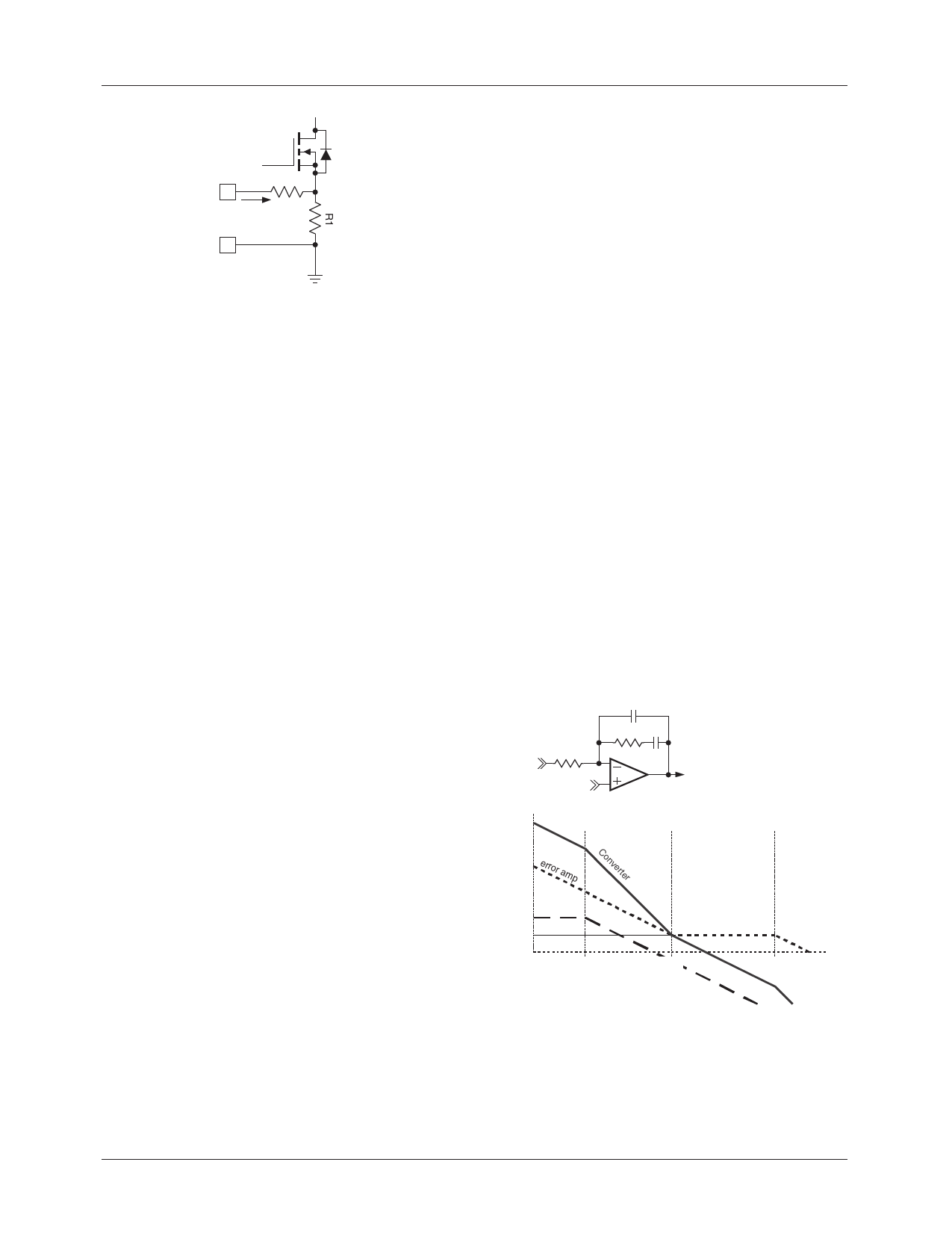
Frequency Loop Compensation
Due to the implemented current mode control, the modulator
has a single pole response with -1 slope at frequency deter-
mined by load
FPO = 2----π----R--1--O---C-----O-
(7)
where RO is load resistance, CO is load capacitance. For this
type of modulator, Type 2 compensation circuit is usually
sufficient. To reduce the number of external components and
simplify the design task, the PWM controller has an inter-
nally compensated error amplifier. Figure 6 shows a Type 2
amplifier and its response along with the responses of a
current mode modulator and of the converter. The Type 2
amplifier, in addition to the pole at the origin, has a zero-pole
pair that causes a flat gain region at frequencies between the
zero and the pole.
C2
R2 C1
R1
VIN
REF
EA Out
error amp
Converter
modulator
18
14
0
F
F
F
P0
Z
P
Figure 6. Compensation
FZ = -2---π----R-1---2--C-----1 = 6kHz
(8a)
FP = -2---π----R-1---2--C-----2 = 600kHz
(8b)
REV. 1.0.10 5/3/04
Share Link: 