FAN5234 查看數據表(PDF) - Fairchild Semiconductor
零件编号
产品描述 (功能)
比赛名单
FAN5234 Datasheet PDF : 15 Pages
| |||
FAN5234
PRODUCT SPECIFICATION
This region is also associated with phase ‘bump’ or reduced
phase shift. The amount of phase shift reduction depends the
width of the region of flat gain and has a maximum value of
90 degrees. To further simplify the converter compensation,
the modulator gain is kept independent of the input voltage
variation by providing feed-forward of VIN to the oscillator
ramp.
The zero frequency, the amplifier high frequency gain and
the modulator gain are chosen to satisfy most typical appli-
cations. The crossover frequency will appear at the point
where the modulator attenuation equals the amplifier high
frequency gain. The only task that the system designer has to
complete is to specify the output filter capacitors to position
the load main pole somewhere within one decade lower than
the amplifier zero frequency. With this type of compensation
plenty of phase margin is easily achieved due to zero-pole
pair phase ‘boost’.
Conditional stability may occur only when the main load
pole is positioned too much to the left side on the frequency
axis due to excessive output filter capacitance. In this case,
the ESR zero placed within the 10kHz...50kHz range gives
some additional phase ‘boost’. Fortunately, there is an oppo-
site trend in mobile applications to keep the output capacitor
as small as possible.
Protection
The converter output is monitored and protected against
extreme overload, short circuit, over-voltage and under-
voltage conditions.
A sustained overload on an output sets the PGOOD pin low
and latches-off the whole chip. Operation can be restored by
cycling the VCC voltage or by toggling the EN pin.
If VOUT drops below the under-voltage threshold, the chip
shuts down immediately.
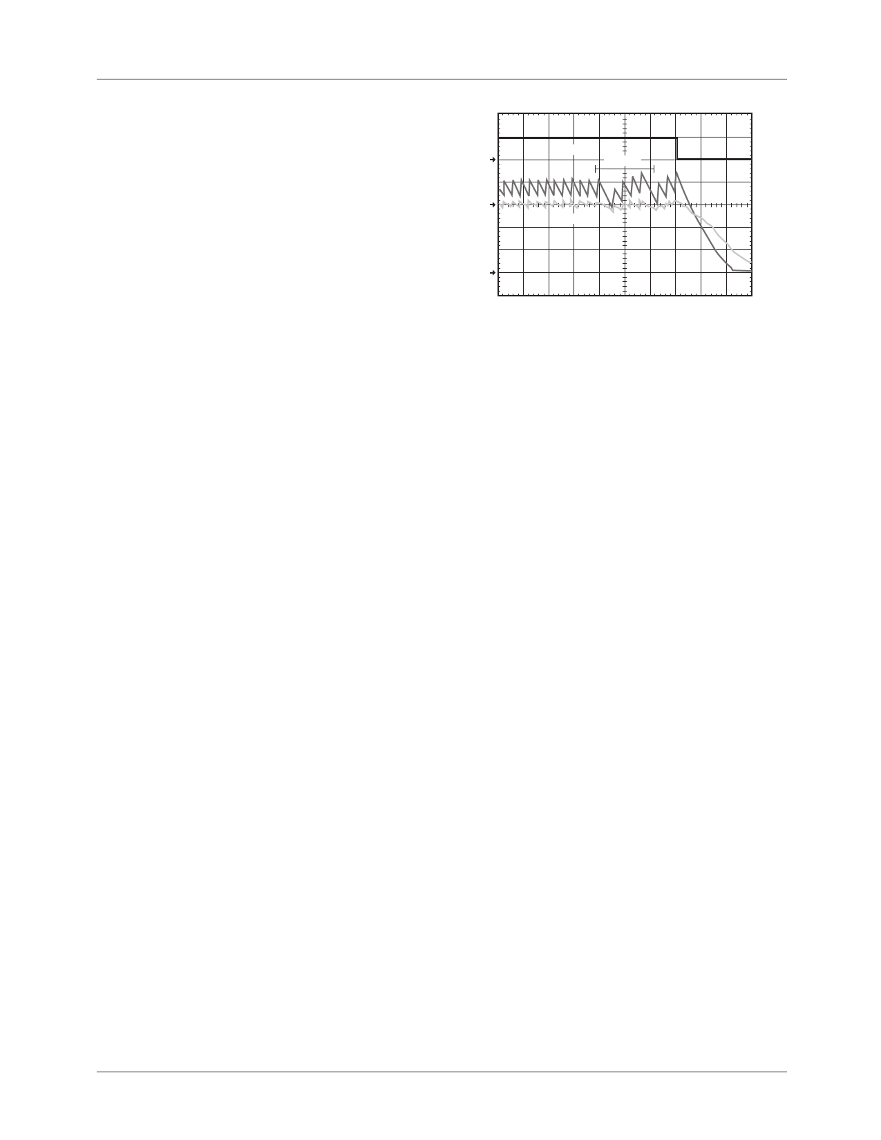
Over-Current sensing
If the circuit's current limit signal (“ILIM det” as shown in
Figure 4) is high at the beginning of a clock cycle, a
pulse-skipping circuit is activated and HDRV is inhibited.
The circuit continues to pulse skip in this manner for the next
8 clock cycles. If at any time from the 9th to the 16th clock
cycle, the "ILIM det" is again reached, the over-current
protection latch is set, disabling the chip. If "ILIM det" does
not occur between cycle 9 and 16, normal operation is
restored and the over-current circuit resets itself.
1
IL
2
PGOOD
8 CLK
VOUT
3
CH1 5.0V
CH3 2.0AΩ
CH2 100mV
M 10.0µs
Figure 7. Over-Current protection waveforms
Over-Voltage / Under-Voltage Protection
Should the VSEN voltage exceed 120% of VREF (0.9V) due
to an upper MOSFET failure, or for other reasons, the
overvoltage protection comparator will force LDRV high.
This action actively pulls down the output voltage and, in the
event of the upper MOSFET failure, will eventually blow the
battery fuse. As soon as the output voltage drops below the
threshold, the OVP comparator is disengaged.
This OVP scheme provides a ‘soft’ crowbar function which
helps to tackle severe load transients and does not invert the
output voltage when activated — a common problem for
latched OVP schemes.
Similarly, if an output short-circuit or severe load transient
causes the output to droop to less than 75% of its regulation
set point. Should this condition occur, the regulator will shut
down.
Over-Temperature Protection
The chip incorporates an over temperature protection circuit
that shuts the chip down when a die temperature of about
150˚C is reached. Normal operation is restored at die tem-
perature below 125˚C with internal Power On Reset asserted,
resulting in a full soft-start cycle.
Design and Component Selection
Guidelines
As an initial step, define operating input voltage range,
output voltage, minimum and maximum load currents for the
controller.
For the examples in the following discussion, we will be
selecting components for:
VIN from 5V to 20V
VOUT = 1.8V @ ILOAD(MAX) = 3.5A
REV. 1.0.10 5/3/04
9
Share Link: 