IDT7024 查看數據表(PDF) - Integrated Device Technology
零件编号
产品描述 (功能)
比赛名单
IDT7024 Datasheet PDF : 22 Pages
| |||
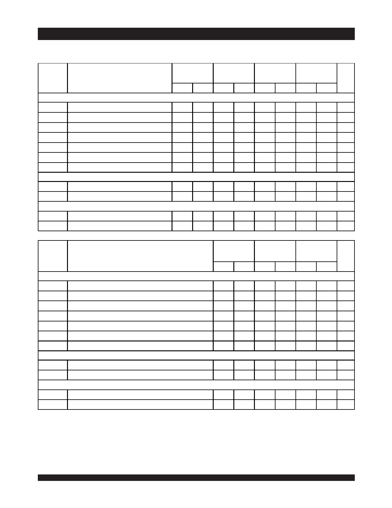
IDT7024S/L
High-Speed 4K x 16 Dual-Port Static RAM
Military, Industrial and Commercial Temperature Ranges
AC Electrical Characteristics Over the
Operating Temperature and Supply Voltage Range(6)
7024X15
Com'l Only
7024X17
Com'l Only
7024X20
Com'l, Ind
& Military
7024X25
Com'l &
Military
Symbol
BUSY TIMING (M/S = VIH)
Parameter
tBAA
BUSY Access Time from Address Match
tBDA
BUSY Disable Time from Address Not Match
tBAC
BUSY Access Time from Chip Enable Low
tBDC
BUSY Disable Time from Chip Enable High
tAPS
Arbitration Priority Set-up Time(2)
tBDD
BUSY Disable to Valid Data(3)
tWH
Write Hold After BUSY(5)
BUSY INPUT TIMING (M/S = VIH)
tWB
BUSY Input to Write(4)
tWH
Write Hold After BUSY(5)
Min. Max. Min. Max. Min. Max. Min. Max. Unit
____
15
____
17
____
20
____
20
ns
____
15
____
17
____
20
____
20
ns
____
15
____
17
____
20
____
20
ns
____
15
____
17
____
17
____
17
ns
5
____
5
____
5
____
5
____
ns
____
18
____
18
____
30
____
30
ns
12
____
13
____
15
____
17
____
ns
0
____
12
____
0
____
13
____
0
____
15
____
0
____
ns
17
____
ns
PORT-TO-PORT DELAY TIMING
tWDD
Write Pulse to Data Delay(1)
tDDD
Write Data Valid to Read Data Delay(1)
____
30
____
30
____
45
____
50
ns
____
25
____
25
____
35
____
35
ns
2740 tbl 14a
7024X35
Com'l &
Military
7024X55
Com'l, Ind
& Military
7024X70
Military Only
Symbol
Parameter
BUSY TIMING (M/S = VIH)
tBAA
BUSY Access Time from Address Match
tBDA
BUSY Disable Time from Address Not Match
tBAC
BUSY Access Time from Chip Enable Low
Min. Max. Min. Max. Min. Max. Unit
____
20
____
45
____
45
ns
____
20
____
40
____
40
ns
____
20
____
40
____
40
ns
tBDC
BUSY Disable Time from Chip Enable High
tAPS
Arbitration Priority Set-up Time(2)
tBDD
BUSY Disable to Valid Data(3)
tWH
Write Hold After BUSY(5)
BUSY INPUT TIMING (M/S = VIH)
tWB
BUSY Input to Write(4)
tWH
Write Hold After BUSY(5)
____
20
____
35
____
35
ns
5
____
5
____
5
____
ns
____
35
____
40
____
45
ns
25
____
25
____
25
____
ns
0
____
0
____
0
____
ns
25
____
25
____
25
____
ns
PORT-TO-PORT DELAY TIMING
tWDD
Write Pulse to Data Delay(1)
tDDD
Write Data Valid to Read Data Delay(1)
____
60
____
80
____
95
ns
____
45
____
65
____
80
ns
NOTES:
1. Port-to-port delay through RAM cells from writing port to reading port, refer to "Timing Waveform of Write Port-to-Port Read and BUSY (M/S = VIH)".
2. To ensure that the earlier of the two ports wins.
3. tBDD is a calculated parameter and is the greater of 0ns, tWDD – tWP (actual) or tDDD – tDW (actual).
4. To ensure that the write cycle is inhibited on port 'B' during contention with port 'A'.
5. To ensure that a write cycle is completed on port 'B' after contention with port 'A'.
6. 'X' in part number indicates power rating (S or L).
2740 tbl 14b
61.432
Share Link: 