LIS3L02DQ 查看數據表(PDF) - STMicroelectronics
零件编号
产品描述 (功能)
比赛名单
LIS3L02DQ Datasheet PDF : 19 Pages
| |||
LIS3L02DQ
Transfer when Master is writing multiple bytes to slave:
Master ST SAD + W
SUB
Slave
SAK
SAK
DATA
SAK
DATA
SP
SAK
Transfer when Master is receiving (reading) one byte of data from slave:
Master ST SAD + W
SUB
SR SAD + R
Slave
SAK
SAK
SAK
DATA
NMAK SP
Transfer when Master is receiving (reading) multiple bytes of data from slave
Master ST SAD + W
SUB
SR SAD + R
Slave
SAK
SAK
SAK
DATA
MAK
Master SR
Slave
DATA
MAK
DATA
NMAK SP
Data are transmitted in byte format. Each data transfer contains 8 bits. The number of bytes transferred
per transfer is unlimited. Data is transferred with the Most Significant Bit (MSB) first. If a receiver can’t re-
ceive another complete byte of data until it has performed some other function, it can hold the clock line,
SCL LOW to force the transmitter into a wait state. Data transfer only continues when the receiver is ready
for another byte and releases the data line. If a slave receiver doesn’t acknowledge the slave address (i.e.
it is not able to receive because it is performing some real time function) the data line must be left HIGH
by the slave. The Master can then abort the transfer. A LOW to HIGH transition on the SDA line while the
SCL line is HIGH is defined as a STOP condition. Each data transfer must be terminated by the generation
of a STOP condition.
In order to read multiple bytes, it is necessary to assert the most significant bit of the sub-address field. In
other words, SUB(7) must be equal to 1 while SUB(6-0) represents the address of first register to read.
4.2 SPI Bus Interface
The SPI interface present inside the LIS3L02DQ is a bus slave. The SPI allows to write and read the reg-
isters of the device. The Serial Interface interacts with the outside world with 4 wires: CS, SPC, SPDI and
SPDO.
4.2.1 Read & Write registers
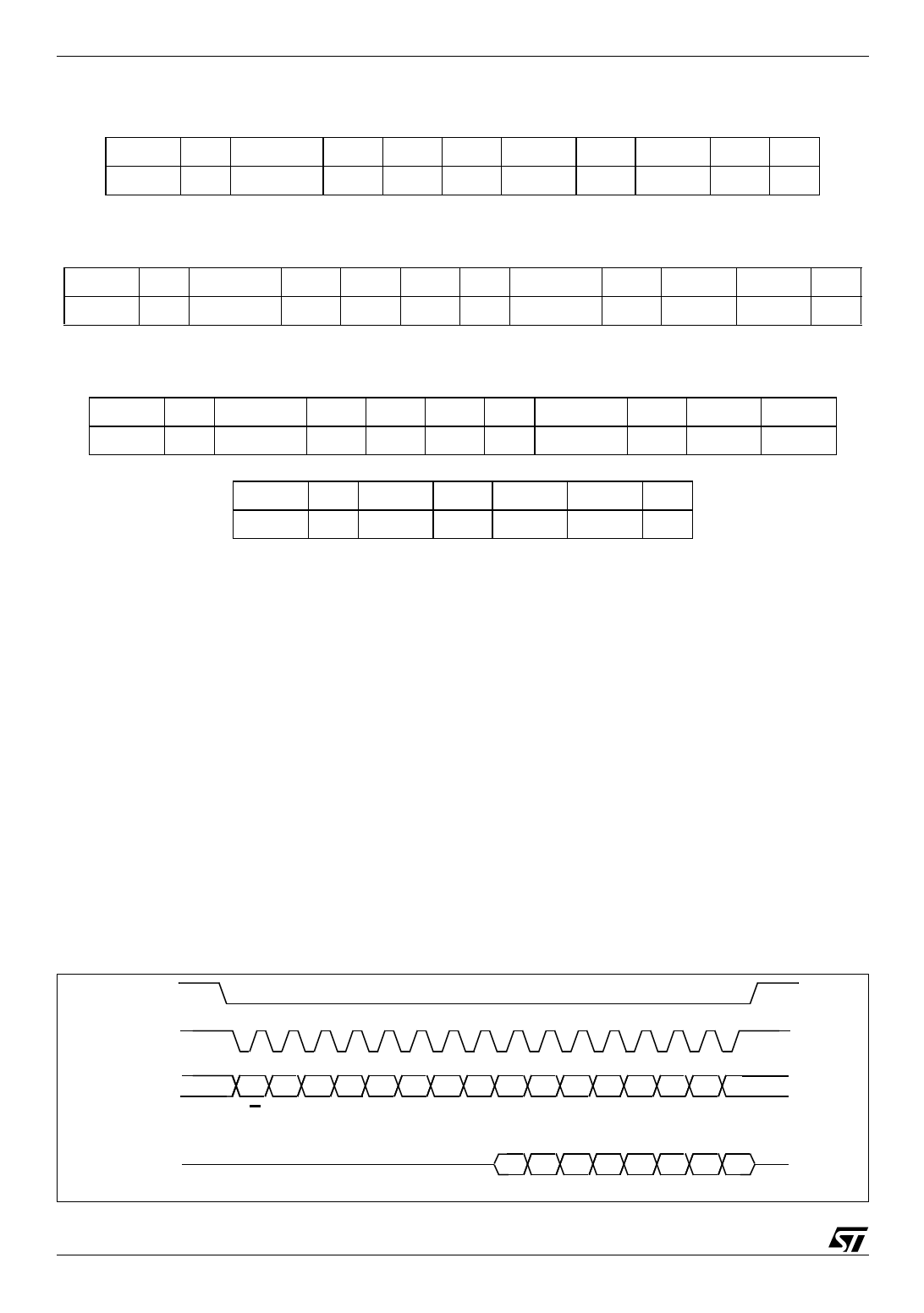
Figure 5. Read & write protocol
CS
SPC
SPDI
SPDO
RW
DI7 DI6 DI5 DI4 DI3 DI2 DI1 DI0
AD6 AD5 AD4 AD3 AD2 AD1 AD0
DO7 DO6 DO5 DO4 DO3 DO2 DO1 DO0
8/19
Share Link: 