M37640E8FP 查看數據表(PDF) - Mitsumi
零件编号
产品描述 (功能)
比赛名单
M37640E8FP Datasheet PDF : 96 Pages
| |||
Ver 1.4
MITSUBISHI MICROCOMPUTERS
7640 Group
SINGLE-CHIP 8-BIT CMOS MICROCOMPUTER
1.19 UART
This chip contains two identical UARTs. Each UART
has the following main features:
• Clock selection .................................. F or SCSGCLK
• Prescaler selection ............... x1/x8/x32/x256 divisions
............................................ (both F and SCSGCLK)
• Baud rate .......................................... (at F = 12MHz)
......................... 11.4 bits/second-750 Kbytes/second
• Error detection ...................................... parity/framing/
...................................................... overrun/error sum
• Parity .................................................. odd/even/none
• Stop bits ........................................................... 1 or 2
• Character length .................................... 7, 8, or 9 bits
• Transmit/receive buffer .................................. 2 stages
...................................................... (double buffering)
• Handshaking ............................... Clear-to-Send (CTS)
............................................. Request-to-Send (RTS)
• Interrupt generation conditions ............. Transmit Buffer
..................................... Empty or Transmit Complete
........................................................... Receive Buffer
.................................................... Receive Error Sum
• Address ............... mode for multi-receiver environment
The following descriptions apply to both UARTs.
The UART receives parallel data from the core or
DMAC, converts it into serial data, and transmits the
results to the send data output terminal UTXDx. The
UART receives serial data from an external source
through the receive data input URXDx, converts it into
parallel data, and makes it available to the core or
DMAC. The UART can detect parity, overrun, and
framing errors in the input stream and report the appro-
priate status information. A double buffering
configuration is used for the UART’s transmit and re-
ceive operations. This double buffering is
accomplished by the use of a transmit buffer and
transmit shift register on the transmit side and the re-
ceive buffer and receive shift register on the receive
side.
The UART supports an address mode for use in a
multi-receiver environment where an address is sent
before each message to designate which UART or
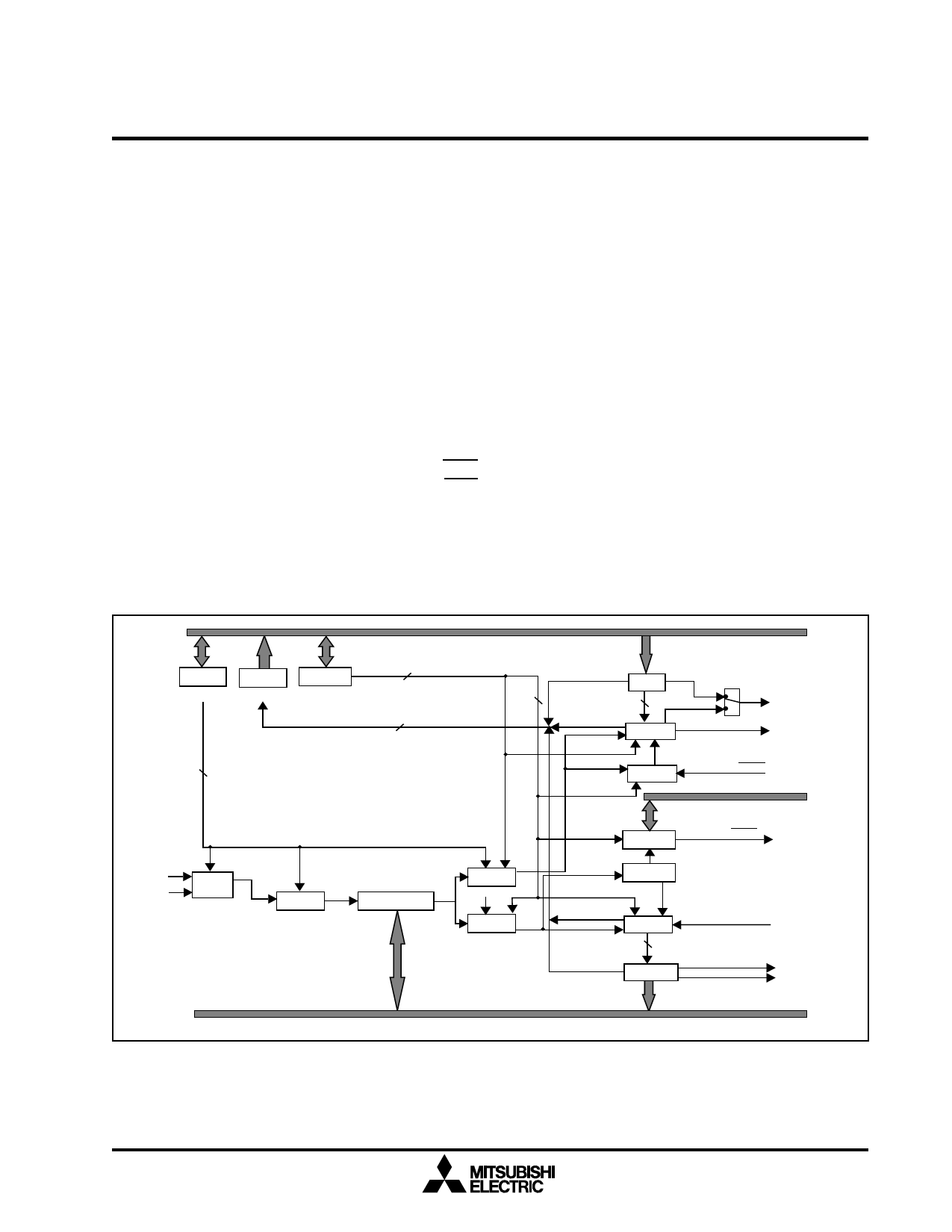
UARTs are to wake-up and receive the message. Fig-
ure 1.41 is a block diagram of the UART. It is valid for
both UART1 and UART2.
Data Bus
UART Mode
Register
UxMOD
UART Status
Register
UxSTS
UART Control
Register
UxCON
Tx Enable
Tx Buffer Empty Transmit TBE
Buffer
TIS = "0"
Tx Complete
Transmit
Shift Register
Transmit Interrupt
TCM
TIS = "1"
Transmit line to UTXDx
CLKSEL
Φ
SCSGCLK Clock Set
PS 1,0
Prescaler
/1/8/32/256
LE 1,0; PEN; STB
Baud Rate Generator
Data Format
Bit Counter
LE 1,0; PEN; STB
Data Format
Bit Counter
___
CTS_SEL
ST/STP/PA
Generator
___
RTS_SEL RTS Control
Register
From CTSx
Data Bus
To RTSx
Rx Enable
Stop and Start
Detect
Rx Status Errors
Receive
Shift Register
Receive line from URXDx
Rx Complete Receive
Buffer Register
Receive Buffer Full Interrupt
Receive Error Interrupt
Data Bus
Fig. 1.41. UART Block Diagram
41
Share Link: 