PDI1394P25BY 查看數據表(PDF) - Philips Electronics
零件编号
产品描述 (功能)
比赛名单
PDI1394P25BY Datasheet PDF : 42 Pages
| |||
Philips Semiconductors
1-port 400 Mbps physical layer interface
Product data
PDI1394P25BY
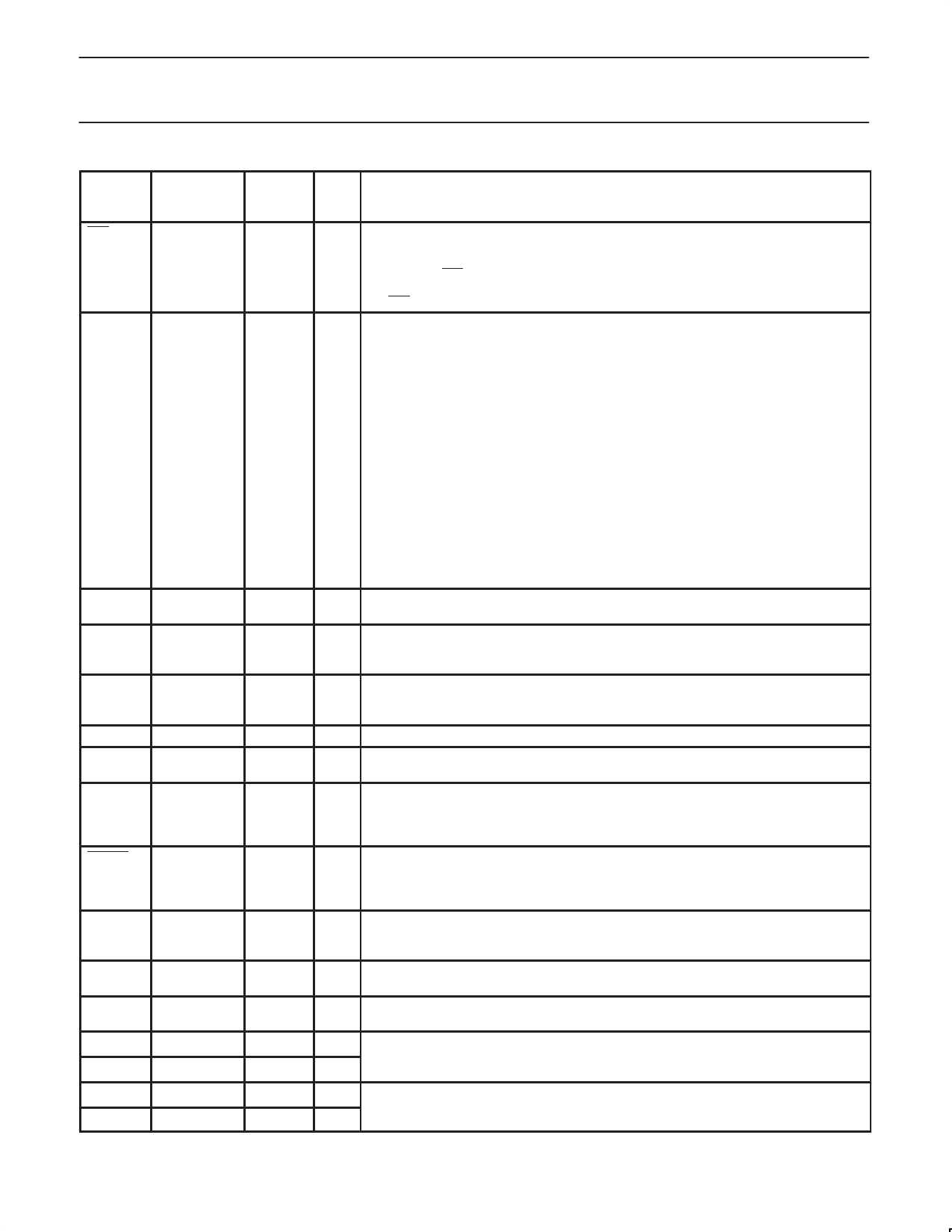
Name
Pin Type
LQFP
I/O
Pin
Numbers
Description
ISO
CMOS
19
I Link interface isolation control input. This terminal controls the operation of output
differentiation logic on the CTL and D terminals. If an optional isolation barrier of the type
described in Annex J of IEEE Std 1394–1995 is implemented between the PDI1394P25
and LLC, the ISO terminal should be tied low to enable the differentiation logic. If no
isolation barrier is implemented (direct connection), or bus holder isolation is implemented,
the ISO terminal should be tied high to disable the differentiation logic.
LPS
CMOS 5 V tol 13
I Link Power Status input. This terminal is used to monitor the active/power status of the
link layer controller and to control the state of the PHY-LLC interface. This terminal should
be connected to either the VDD supplying the LLC through a 10 kΩ resistor, or to a pulsed
output which is active when the LLC is powered. A pulsed signal should be used when an
isolation barrier exists between the LLC and PHY. (See Figure 8)
The LPS input is considered inactive if it is sampled low by the PHY for more than 2.6 µs
(128 SYSCLK cycles), and is considered active otherwise (i.e., asserted steady high or an
oscillating signal with a low time less than 2.6 µs). The LPS input must be high for at least
21 ns in order to be guaranteed to be observed as high by the PHY.
When the PDI1394P25 detects that LPS is inactive, it will place the PHY-LLC interface
into a low-power reset state. In the reset state, the CTL and D outputs are held in the logic
zero state and the LREQ input is ignored; however, the SYSCLK output remains active. If
the LPS input remains low for more than 26 µs (1280 SYSCLK cycles), the PHY-LLC
interface is put into a low-power disabled state in which the SYSCLK output is also held
inactive. The PHY-LLC interface is placed into the disabled state upon hardware reset.
The LLC is considered active only if both the LPS input is active and the LCtrl register bit
is set to 1, and is considered inactive if either the LPS input is inactive or the LCtrl register
bit is cleared to 0.
LREQ
CMOS 5 V tol 48
I LLC Request input. The LLC uses this input to initiate a service request to the
PDI1394P25. Bus holder is built into this terminal.
NC
No connect 22, 38,
— These pins are not internally connected and consequently are “don’t cares”. Other
39
vendors’ pin compatible chips may require connections and external circuitry on
these pins.
PC0
CMOS 5 V tol 16
PC1
17
PC2
18
I Power Class programming inputs. On hardware reset, these inputs set the default value of
the power class indicated during self-ID. Programming is done by tying the terminals high
or low. Refer to Table 21 for encoding.
PD
CMOS 5 V tol 12
I Power Down input. A logic high on this terminal turns off all internal circuitry.
PLLGND
Supply
41
— PLL circuit ground terminals. These terminals should be tied together to the low
impedance circuit board ground plane.
PLLVDD
Supply
40
— PLL circuit power terminals. A combination of high frequency decoupling capacitors near
each terminal are suggested, such as paralleled 0.1 µF and 0.001 µF. These supply
terminals are separated from DVDD and AVDD internal to the device to provide noise
isolation. They should be tied at a low impedance point on the circuit board.
RESET CMOS 5 V tol 37
I Logic reset input. Asserting this terminal low resets the internal logic. An internal pull-up
resistor to VDD is provided so only an external delay capacitor is required for proper
power-up operation. For more information, refer to Section 17.2. This input is otherwise a
standard Schmitt logic input, and can also be driven by an open-drain type driver.
R0
Bias
33
— Current setting resistor pins These pins are connected to an external resistance to set the
R1
34
internal operating currents and cable driver output currents. A resistance of 6.34 kΩ ±1%
is required to meet the IEEE 1394–1995 Std. output voltage limits.
SYSCLK
CMOS
1
O System clock output. Provides a 49.152 MHz clock signal, synchronized with data
transfers, to the LLC.
TEST0
CMOS
24
I Test control input. This input is used in manufacturing tests of the PDI1394P25. For
normal use, this terminal should be tied to GND.
TPA0+
TPA0–
Cable
30
Cable
29
I/O Twisted-pair cable A differential signal terminals. Board traces from each pair of positive
and negative differential signal terminals should be kept matched and as short as possible
I/O to the external load resistors and to the cable connector.
TPB0+
TPB0–
Cable
28
Cable
27
I/O Twisted-pair cable B differential signal terminals. Board traces from each pair of positive
and negative differential signal terminals should be kept matched and as short as possible
I/O to the external load resistors and to the cable connector.
2002 Oct 11
5
Share Link: 