UPC1935 查看數據表(PDF) - NEC => Renesas Technology
零件编号
产品描述 (功能)
比赛名单
UPC1935 Datasheet PDF : 28 Pages
| |||
µ PC1935
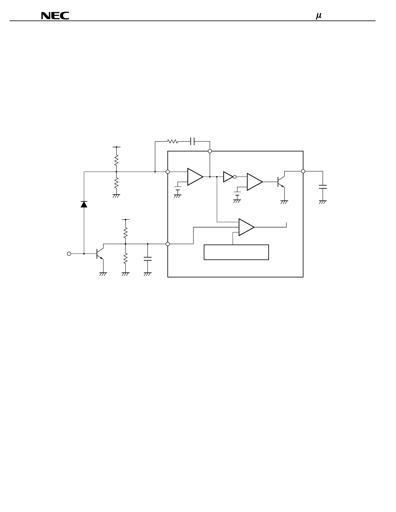
3.5.2 Channel 2 (for step-up)
The ON/OFF signal control method of the output oscillation of channel 2 is to input the ON/OFF signal from ON2 as
shown in Figure 3-4. The PWM converter can be turned ON/OFF by controlling the level of the DTC2 pin. However, it is
necessary to keep the level of the FB2 output low (the SCP comparator input high) so that the timer latch does not start
when the PWM converter is OFF. In this circuit example, the FB2 output level is controlled by controlling the level of the II2
pin.
Figure 3-4 ON/OFF Control (channel 2: step-up)
VO2
(Converter
output
R21
voltage)
R22
D21
VREF
R23
ON2
Q21
R24
C21
FB2
II2
–
+ Error
0.3 V amplifier
SCP comparator
(common to each channel) DLY
+
Q1
–
0.63 V
DTC2
To output stage
+
+
–
PWM comparator
Oscillation section
(common to each channel)
CDLY
(1) When ON2 is high: OFF status
Q21: ON → DTC2 pin: Low level → Output duty of PWM comparator: 0 %
D21: ON → II2 pin: High level → FB2 output: Low level → SCP comparator output: High level → Timer latch stops.
(2) When ON2 is low: ON status
Q21: OFF → C21 is charged in the sequence of [VREF → R23 → C21] → DTC2 pin voltage rises → Soft start
D21: OFF → II2 pin: Low level → FB2 output: High level → SCP comparator output: Low level → Q1 is OFF
→ Charging CDLY starts (timer latch start).
Caution Keep the low-level voltage of the DTC2 pin within 1.2 V and the high-level voltage of the II2 pin at
0.3 V or higher. The maximum voltage that is applied to the II2 pin must be equal to or lower than
VREF.
18
Data Sheet G13418EJ3V0DS00
Share Link: 