L3GD20 查看數據表(PDF) - STMicroelectronics
零件编号
产品描述 (功能)
比赛名单
L3GD20 Datasheet PDF : 44 Pages
| |||
Mechanical and electrical specifications
L3GD20
2.4.2
I2C - Inter IC control interface
Subject to general operating conditions for Vdd and Top.
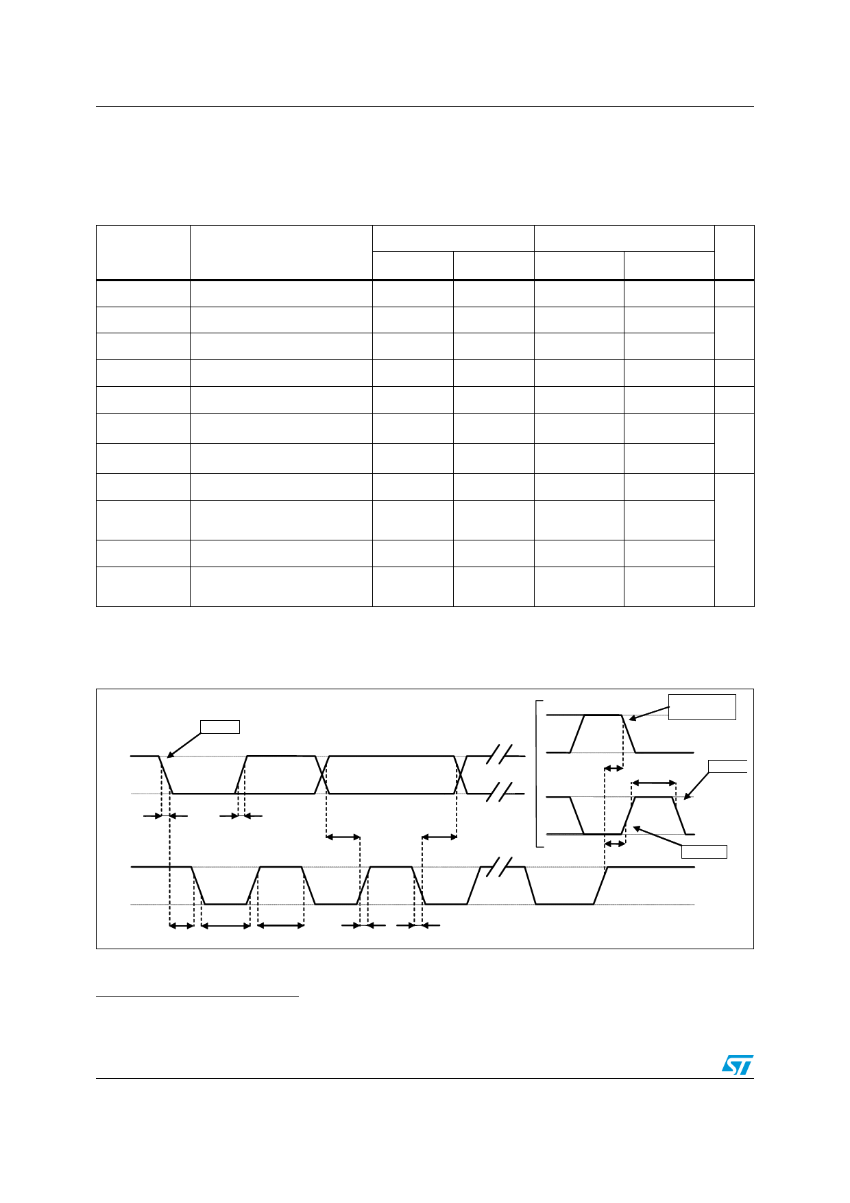
Table 7. I2C slave timing values (TBC)
Symbol
Parameter
I2C standard mode(1)
Min
Max
f(SCL)
tw(SCLL)
tw(SCLH)
tsu(SDA)
th(SDA)
SCL clock frequency
SCL clock low time
SCL clock high time
SDA setup time
SDA data hold time
0
100
4.7
4.0
250
0
3.45
tr(SDA) tr(SCL) SDA and SCL rise time
1000
tf(SDA) tf(SCL) SDA and SCL fall time
300
th(ST)
START condition hold time
4
tsu(SR)
Repeated START condition
setup time
4.7
tsu(SP)
STOP condition setup time
4
tw(SP:SR)
Bus free time between STOP
and START condition
4.7
1. Data based on standard I2C protocol requirement; not tested in production.
2. Cb = total capacitance of one bus line, in pF.
I2C fast mode (1)
Min
Max
0
400
1.3
0.6
100
0
0.9
20 + 0.1Cb (2)
300
20 + 0.1Cb (2)
300
0.6
0.6
0.6
1.3
Unit
kHz
µs
ns
µs
ns
µs
Figure 4. I2C slave timing diagram (b)
67$57
6'$
5(3($7('
67$57
WVX
65
WZ
63
65
67$57
WI
6'$
6&/
WU
6'$
WVX
6'$
WK
6'$
WVX
63
6723
WK
67
WZ
6&//
WZ
6&/+
WU
6&/
WI
6&/
!-V
b. Measurement points are at 0.2·Vdd_IO and 0.8·Vdd_IO, for both ports.
12/44
Doc ID 022116 Rev 1
Share Link: 