M37640E8FP 查看數據表(PDF) - Mitsumi
零件编号
产品描述 (功能)
比赛名单
M37640E8FP Datasheet PDF : 96 Pages
| |||
Ver 1.4
MITSUBISHI MICROCOMPUTERS
7640 Group
SINGLE-CHIP 8-BIT CMOS MICROCOMPUTER
1.15 INTERRUPT CONTROL UNIT
This section details a specialized peripheral, the inter-
rupt control unit (ICU).
This series supports a maximum of 23 maskable inter-
rupts, one software interrupts, and one reset vector
that is treated as a non-maskable interrupt.
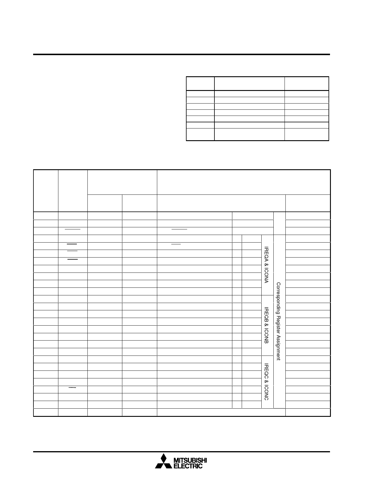
Table 1.6 describes the interrupt registers. See Table
1.7 for the interrupt sources, jump destination ad-
dresses, interrupt priorities, and section references
for the interrupt request sources.
Table 1.6. Interrupt Registers
Address
Description
000216
000316
000416
000516
000616
000716
001116
Interrupt request register A
Interrupt request register B
Interrupt request register C
Interrupt control register A
Interrupt control register B
Interrupt control register C
Interrupt polarity selection
register
Table 1.7. Interrupt Vector
Priority
1
2
3
4
5
6
7
8
9
10
11
12
13
14
15
16
17
18
19
20
21
22
23
24
25
26
27
Interrupt
RSRV1
RSRV2
RESET
USB
SOF
INT0
INT1
DMA1
DMA2
U1RBF
U1TX
U1ES
U2RBF
U2TX
U2ES
TX
TY
T1
T2
T3
CNTR0
CNTR1
SIO
IBF
OBE
KEY
BRK
Jump Destination
Storage Address
(Vector Address)
High-order Low-order
Byte
Byte
FFFF
FFFE
FFFD
FFFC
FFFB
FFFA
FFF9
FFF8
FFF7
FFF6
FFF5
FFF3
FFF4
FFF2
FFF1
FFF0
FFEF
FFED
FFEE
FFEC
FFEB
FFEA
FFE9
FFE7
FFE8
FFE6
FFE5
FFE4
FFE3
FFE2
FFE1
FFE0
FFDF
FFDE
FFDD
FFDC
FFDB
FFDA
FFD9
FFD8
FFD7
FFD6
FFD5
FFD4
FFD3
FFD2
FFD1
FFD0
FFCF
FFCE
FFCD
FFCC
FFCB
FFCA
Remarks
Reserved for factory use
Reserved for factory use
User RESET (Non-Maskable)
USB Function Interrupt
0
USB SOF Interrupt
1
External Interrupt 0
2
External Interrupt 1
3
DMAC Channel 0 Interrupt
4
DMAC Channel 1 Interrupt
5
UART1 Receiver Buffer Full
6
UART1 Transmit Interrupt
7
UART1 Error Sum Interrupt
0
UART2 Receiver Buffer Full
1
UART2 Transmit Interrupt
2
UART2 Error Sum Interrupt
3
Timer X Interrupt
4
Timer Y Interrupt
5
Timer 1 Interrupt
6
Timer 2 Interrupt
7
Timer 3 Interrupt
0
External CNTR0 Interrupt
1
External CNTR1 Interrupt
2
SIO Interrupt
3
Input Buffer Full Interrupt
4
Output Buffer Empty Interrupt
5
Key-on Wake Up
6
BRK Instruction (Non-Maskable)
LSB
MSB
LSB
MSB
LSB
MSB
Acronym and
Value at Reset
IREQA=00
IREQB=00
IREQC=00
ICONA=00
ICONB=00
ICONC=00
IPOL=00
Reference
Section 1.21.2.1
Section 1.21.2.2
Section 1.15.1
Section 1.15.1
Section 1.23
Section 1.23
Section 1.19.4.2
Section 1.19.4.1
Section 1.19.4.2
Section 1.19.4.2
Section 1.19.4.1
Section 1.19.4.2
Section 1.17
Section 1.17
Section 1.17
Section 1.17
Section 1.17
Section 1.17.1.2
Section 1.17.2
Section 1.18
Section 1.22
Section 1.22
Section 1.16
26
Share Link: 