M37640E8FP 查看數據表(PDF) - Mitsumi
零件编号
产品描述 (功能)
比赛名单
M37640E8FP Datasheet PDF : 96 Pages
| |||
Ver 1.4
MITSUBISHI MICROCOMPUTERS
7640 Group
SINGLE-CHIP 8-BIT CMOS MICROCOMPUTER
MSB ICA7
ICA6
ICA5
ICA4 ICA3
ICA2
ICA1
ICA0
LSB Address: 000516
0
Access: R/W
Reset:
0016
ICA 0
ICA 1
ICA 2
ICA 3
ICA 4
ICA 5
ICA 6
ICA 7
USB Function Interrupt Enable (bit 0)
USB SOF Interrupt Enable (bit 1)
External Interrupt 0 Enable (bit 2)
External Interrupt 1 Enable (bit 3)
DMAC channel 0 Interrupt Enable (bit 4)
DMAC channel 1 Interrupt Enable (bit 5)
UART1 Receive Buffer Full Interrupt Enable (bit 6)
UART1 Transmit Interrupt Enable (bit 7)
0: Interrupt Disable
1: Interrupt Enable
Fig. 1.27 Interrupt Control Register A (ICONA)
MSB
7
ICB7
ICB6
ICB5
ICB4 ICB3
ICB2
Fig. 1.28. Interrupt Control Register B (ICONB)
ICB1
ICB0
LSB Address: 000616
0
Access: R/W
Reset:
0016
ICB 0
ICB 1
ICB 2
ICB 3
ICB 4
ICB 5
ICB 6
ICB 7
UART1 Error Sum Interrupt Enable (bit 0)
UART2 Receive Buffer Full Interrupt Enable (bit 1)
UART2 Transmit Interrupt Enable (bit 2)
UART2 Error Sum Interrupt Enable (bit 3)
Timer X Interrupt Enable (bit 4)
Timer Y Interrupt Enable (bit 5)
Timer 1 Interrupt Enable ( bit 6)
Timer 2 Interrupt Enable (bit 7)
0: Interrupt Disable
1: Interrupt Enable
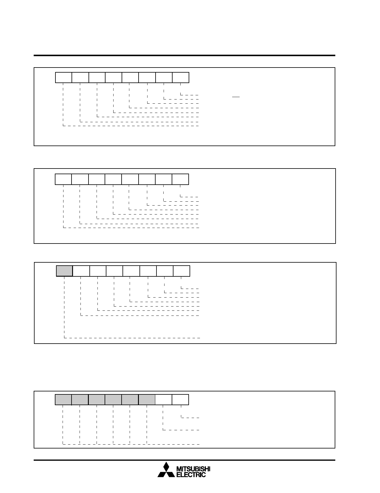
MSB
7
Reserved ICC6
ICC5
ICC4 ICC3
ICC2
Fig. 1.29. Interrupt Control Register C (ICONC)
ICC1
ICC0
LSB Address: 000716
0 Access: R/W
Reset:
0016
ICC 0
ICC 1
ICC 2
ICC 3
ICC 4
ICC 5
ICC 6
ICC 7
Timer 3 Interrupt Enable (bit 0)
External CNTR0 Interrupt Enable (bit 1)
External CNTR1 Interrupt Enable (bit 2)
SIO Interrupt Enable (bit 3)
Input Buffer Full Interrupt Enable (bit 4)
Output Buffer Empty Interrupt Enable (bit 5)
Key-on Wake up Interrupt Enable (bit 6)
0: Interrupt Disable
1: Interrupt Enable
Reserved (Read/Write “0”)
The interrupt polarity register allows the user to se- request. The polarity register (IPOL) for the external
lect the edge that will trigger an external interrupt interrupts is shown in Figure 1.30.
MSB
7
Reserved Reserved
Reserved
Reserved
Reserved
Reserved
INT1 Pol
INT0 Pol
LSB
0
Address:
Access:
Reset:
001116
R/W
0016
INT0 Pol
INT1 Pol
Bits 2-7
INT0 Interrupt Edge Selection Bit
0: Falling edge selected
1: Rising edge selected
INT1 Interrupt Edge Selection Bit
0: Falling edge selected
1: Rising edge selected
Reserved (Read/Write “0”)
Fig. 1.30. Interrupt Polarity Register (IPOL)
28
Share Link: 